Reduced susceptibility to electrostatic discharge during 3D semiconductor device bonding and assembly

a semiconductor device and susceptibility reduction technology, applied in the field of reducing the susceptibility of electrostatic discharge in stacked ic device assembly, can solve the problem that the semiconductor device may be more susceptible to damage, and achieve the effect of reducing the potential damage to sensitive circuit elements and reducing the electrostatic discharge susceptibility

Inactive Publication Date: 2012-06-12
QUALCOMM INC
View PDF8 Cites 2 Cited by
  • Summary
  • Abstract
  • Description
  • Claims
  • Application Information

AI Technical Summary

Benefits of technology

[0006]A method to reduce electrostatic discharge when assembling a stacked IC device includes coupling a voltage reference plane, usually the ground plane or body, of a first semiconductor device and a voltage reference plane, usually the ground plane or body of a second semiconductor device to substantially the same electrical potential. Active circuitry on the first semiconductor device and active circuitry on the second semiconductor device are electrically coupled after the ground planes are coupled. Electrically coupling the ground planes of the first and the second semiconductor device creates an electrostatic discharge path to ground, thus reducing potential damage to sensitive circuit elements.
[0010]In still another embodiment, a first semiconductor device for assembly with a second semiconductor device to create a stacked IC device includes means for reducing susceptibility to electrostatic discharge (ESD) coupled to a ground plane of the first semiconductor device. The reducing means enables placing of the ground plane of the first semiconductor device and a ground plane of the second semiconductor device at substantially a same electrical potential before coupling active circuitry of the first semiconductor device to active circuitry of the second semiconductor device.

Problems solved by technology

The semiconductor devices may then be more susceptible to damage from ESD during assembly.

Method used


Image

  • Reduced susceptibility to electrostatic discharge during 3D semiconductor device bonding and assembly
  • Reduced susceptibility to electrostatic discharge during 3D semiconductor device bonding and assembly
  • Reduced susceptibility to electrostatic discharge during 3D semiconductor device bonding and assembly

Examples


Embodiment Construction

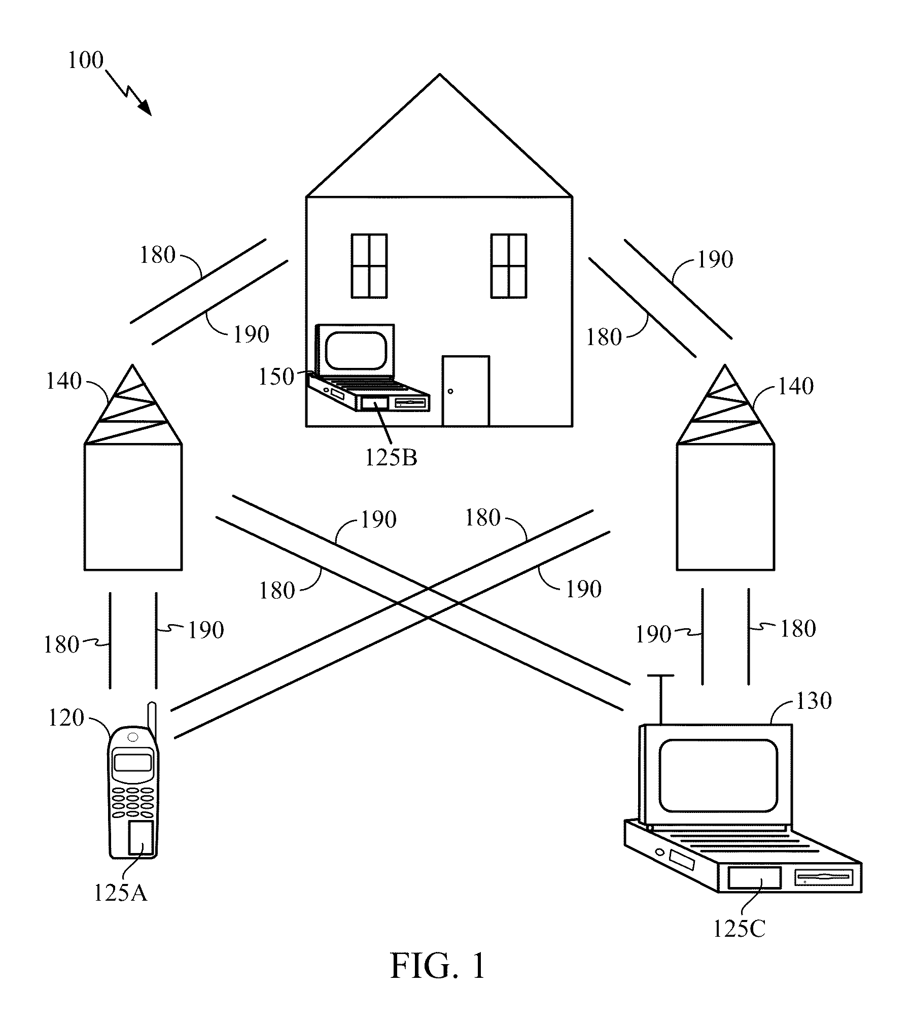
[0018]FIG. 1 shows an exemplary communication system 100 in which an embodiment of the disclosure may be advantageously employed. For purposes of illustration, FIG. 1 shows three remote units 120, 130, and 150 and two base stations 140. It will be recognized that conventional communication systems may have many more remote units and base stations. Remote units 120, 130, and 150 include 3D stacked semiconductor devices 125A, 125B and 125C, which are embodiments of the disclosure as discussed further below. FIG. 1 shows forward link signals 180 from the base stations 140 and the remote units 120, 130, and 150 and reverse link signals 190 from the remote units 120, 130, and 150 to base stations 140.

[0019]In FIG. 1, remote unit 120 is shown as a mobile telephone, remote unit 130 is shown as a portable computer, and remote unit 150 is shown as a fixed location remote unit. For example, the remote units may be cell phones, hand-held personal communication systems (PCS) units, portable dat...


PUM

PropertyMeasurementUnit
conductiveaaaaaaaaaa
perimeteraaaaaaaaaa
areaaaaaaaaaaa

Abstract

A method to reduce electrostatic discharge susceptibility when assembling a stacked IC device. The method includes coupling a ground plane of a first semiconductor device and a ground plane of a second semiconductor device to substantially a same electrical potential. Active circuitry on the first semiconductor device and active circuitry on the second semiconductor device are electrically coupled after the ground planes are coupled. Electrically coupling the ground planes of the first and the second semiconductor device creates a preferred electrostatic discharge path to ground, thus minimizing potential damage to sensitive circuit elements.

Description

TECHNICAL FIELD[0001]The present disclosure generally relates to semiconductor device assembly. More specifically, the present disclosure relates to reducing electrostatic discharge susceptibility in stacked IC device assembly.BACKGROUND[0002]A 3D semiconductor device (or stacked IC device) can contain two or more semiconductor devices stacked vertically so they occupy less space than two or more conventionally arranged semiconductor devices. The stacked IC device is a single integrated circuit built by stacking silicon wafers and / or ICs and interconnecting them vertically so that they behave as a single device.[0003]Conventionally, the stacked semiconductor devices are wired together using input / output ports either at the perimeter of the device or across the area of the device or both. The input / output ports slightly increase the length and width of the assembly. In some new 3D stacks, through-silicon vias (TSVs) completely or partly replace edge wiring by creating vertical connec...

Claims


Application Information

Patent Timeline
Patent Type & Authority Patents(United States)
IPC IPC(8): H01L23/48H01L23/52H01L29/40
CPCH01L21/50H01L23/488H01L25/0657H01L21/67092H01L23/60H01L25/50H01L2225/06513Y10T29/53174H01L2224/16
Inventor HENDERSON, BRIAN M.JALILIZEINALI, REZAGU, SHIQUN
Owner QUALCOMM INC
Why Eureka
Try Eureka