Thin film transistor array substrate for reducing electrostatic discharge damage

a technology of thin film transistors and array substrates, applied in the direction of instruments, semiconductor devices, electrical apparatus, etc., can solve the problems of insufficient layout area, main circuits and devices are vulnerable to electrostatic discharge phenomenon, and display quality defects, so as to reduce electrostatic discharge damage, simplify the layout of tft array substrates, and reduce the effect of electrostatic discharge phenomenon

Active Publication Date: 2007-06-14
WUHAN CHINA STAR OPTOELECTRONICS TECH CO LTD
View PDF3 Cites 3 Cited by
  • Summary
  • Abstract
  • Description
  • Claims
  • Application Information

AI Technical Summary

Benefits of technology

[0013] Accordingly, the present invention is directed to a thin film transistor array substrate for reducing electrostatic discharge damage, wherein the thin film transistor array substrate is capable of reducing electrostatic discharge phenomenon and simplifying the layout of the TFT array substrate to enhance the production efficiency.

Problems solved by technology

So the short-circuit between the data line 140 and the scan line 130 is generated and leads to some defects of display quality such as white lines or black lines shown on a display panel.
In addition, because the lines and devices on the TFT array substrate 100 are so tiny, the main circuits and devices will be vulnerable to the electrostatic discharge phenomenon.
However, the layout of the peripheral area 114 is complicated by utilizing the above-mentioned method, disposing the electrostatic protection devices, so that the area of layout is not enough.
Hence, it has an adverse effect in simplifying the manufacturing process and enhancing the production efficiency.

Method used


Image

  • Thin film transistor array substrate for reducing electrostatic discharge damage
  • Thin film transistor array substrate for reducing electrostatic discharge damage
  • Thin film transistor array substrate for reducing electrostatic discharge damage

Examples


Embodiment Construction

[0033] Various specific embodiments of the present invention are disclosed below, illustrating examples of various possible implementations of the concepts of the present invention. The following description is made for the purpose of illustrating the general principles of the invention and should not be taken in a limiting sense. The scope of the invention is best determined by reference to the appended claims.

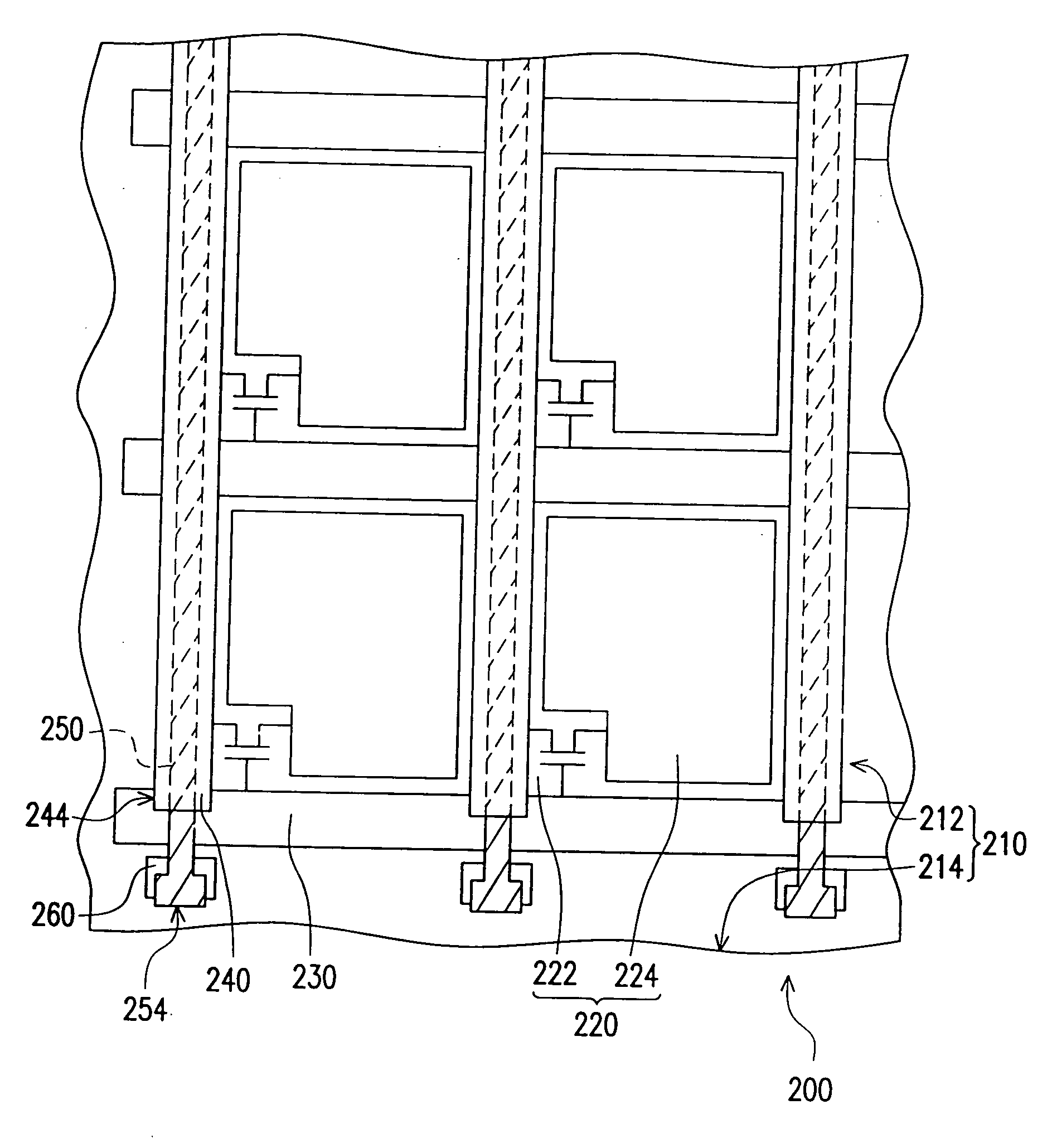
[0034]FIG. 3 is a schematic view of a TFT array substrate according to one preferred embodiment of the present invention. FIG. 4 is an enlarged schematic view of a pixel area in area B shown in FIG. 3. Referring to FIGS. 3 and 4, the conventional TFT array substrate 200 comprises a substrate 210, a plurality of pixel units 220, a plurality of scan lines 230 and a plurality of data lines 240. The substrate 210 has a pixel area 212 and a peripheral area 214 adjacent to the pixel area 212. The pixel units 220 are disposed in the pixel area 212. The scan lines 230 and the data l...


PUM


Abstract

A thin film transistor (TFT) array substrate for reducing electrostatic discharge damage includes a substrate, a plurality of pixel units, scan lines and data lines. The substrate has a pixel area and a peripheral area adjacent to the pixel area. The pixel units are disposed in the pixel area. The scan lines and data lines are disposed in the pixel area of the substrate and electrically connected with the pixel units, wherein one end of each scan line extending to the peripheral area is a bonding pad for the scan line. One end of each data line extending to the peripheral area is a bonding pad for the data line. The other end of each data line extending to the peripheral area is an end part of the data line. Particularly, the end part of the data line does not exceed the outmost scan line.

Description

BACKGROUND OF THE INVENTION [0001] 1. Field of the Invention [0002] The present invention relates to a thin film transistor array substrate. More particularly, the present invention relates to a thin film transistor array substrate which is not be easily damaged by the discharged static electricity. [0003] 2. Description of Related Art [0004] In recent years, with the progressive manufacturing technique in optoelectronics and semiconductor fields, the flat panel display apparatuses are growing rapidly. Wherein the liquid crystal display (LCD) apparatus has become the mainstream in the liquid crystal display apparatuses due to its low operating voltage, low radiation, light weight and thin thickness. [0005] A traditional liquid crystal display (LCD) apparatus mainly comprises a LCD panel and a back light module, wherein the LCD panel generally comprises a thin film transistor (TFT) array substrate, a color filter (CF) array substrate and a liquid crystal layer disposed therebetween. ...

Claims


Application Information

Patent Timeline
Patent Type & Authority Applications(United States)
IPC IPC(8): H01L31/113
CPCG09G3/20G09G2300/08H01L27/124H01L27/0251H01L27/12G09G2330/04
Inventor LIU, WEN-HSIUNGSHEN, HUI-CHUNGHUNG, MENG-FENG
Owner WUHAN CHINA STAR OPTOELECTRONICS TECH CO LTD
Why Eureka
Try Eureka