
CMOS image sensor with multiple stage transfer gate

Inactive Publication Date: 2020-03-26
OMNIVISION TECH INC
View PDF7 Cites 2 Cited by
  • Summary
  • Abstract
  • Description
  • Claims
  • Application Information

AI Technical Summary

Benefits of technology

The patent text discusses three solutions used in the image sensor industry to achieve full electric charge transfer between nodes. However, each solution has its drawbacks. Increasing the electric potential between nodes requires higher power supply voltages, which leads to higher power consumption and specialized processes to manufacture. Additionally, it can cause electrostatic discharge issues. Reducing the conversion gain between nodes can result in more noise and less sensitivity in image sensor operation. Adding additional nodes can require additional contacts and storage nodes for charge to be transferred, which exacerbates the need for increased electric potential of subsequent storage nodes. The patent text proposes a new solution that addresses these drawbacks.

Problems solved by technology

However, this solution typically requires higher power supply voltages to be provided to the image sensor.
The higher power supply voltage may result in higher power consumption, may require specialized processes to manufacture, and / or may require mitigation of electrostatic discharge issues.
However, this solution may result in more noise and less sensitivity in operation of the image sensor.
However, this solution may require additional contacts and storage nodes for charge to be transferred between the stacked silicon chips.

Method used


Image

  • CMOS image sensor with multiple stage transfer gate
  • CMOS image sensor with multiple stage transfer gate
  • CMOS image sensor with multiple stage transfer gate

Examples


Embodiment Construction

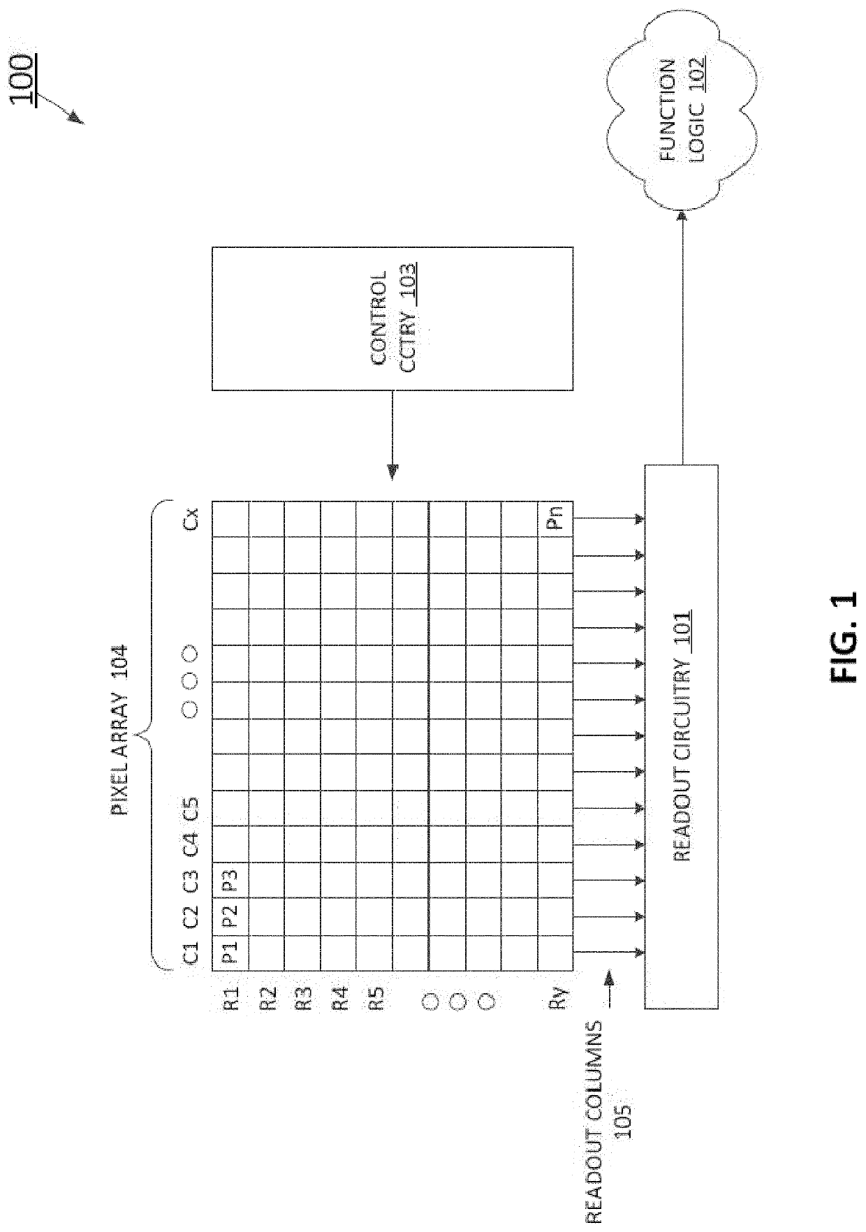
[0010]Examples of an apparatus and method for an image sensor with multiple stage transfer gates are described herein. In the following description, numerous specific details are set forth to provide a thorough understanding of the examples. However, one skilled in the relevant art will recognize that the techniques described herein can be practiced without one or more of the specific details, or with other methods, components, materials, etc. In other instances, well-known structures, materials, or operations are not shown or described in details in order to avoid obscuring certain aspects.

[0011]Reference throughout this specification to “one example” or “one embodiment” means that a particular feature, structure, or characteristic described in connection with the example is included in at least one example of the present invention. Thus, the appearances of the phrases “in one example” or “in one embodiment” in various places throughout this specification are not necessarily all re...


PUM


Abstract

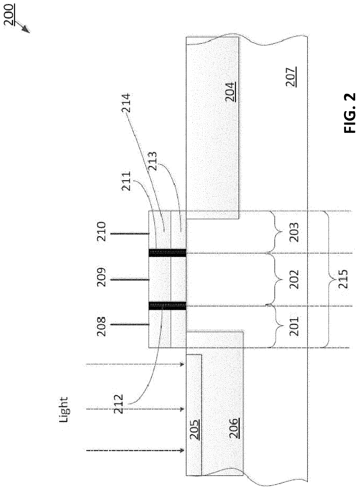
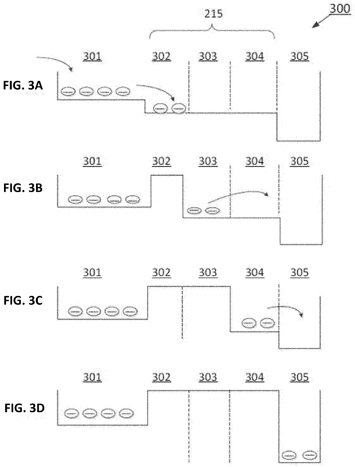
An image sensor pixel comprises a first charge storage node configured to have a first charge storage electric potential; a second charge storage node configured to have a second charge storage electric potential and receive charge from the first charge storage node, wherein the second charge storage electric potential is greater than the first charge storage electric potential; and a transfer circuit coupled between the first and the second charge storage nodes, wherein the transfer circuit comprises at least three transfer regions, wherein: a first transfer region is proximate to the first charge storage node and configured to have a first transfer electric potential greater than the first charge storage electric potential and lower than the second charge storage electric potential; a second transfer region is coupled between the first and a third transfer region and configured to have a second transfer electric potential greater than the first charge storage electric potential and lower than the second charge storage electric potential; and the third transfer region is proximate to the third charge storage node and configured to have a third transfer electric potential greater than the first charge storage electric potential and lower than the second charge storage electric potential. Charges are fully transferred from the first charge storage node to the second charge storage node after a plurality of transfer signal pulses.

Description

TECHNICAL FIELD[0001]This disclosure relates generally to semiconductor image sensors, and in particular but not exclusively, relates to CMOS image sensors with multiple stage transfer gates.BACKGROUND INFORMATION[0002]Image sensors have become ubiquitous. They are widely used in digital still cameras, cellular phones, security cameras, as well as medical, automobile and other applications. The typical global shutter complementary metal oxide semiconductor (CMOS) image sensor is operated as follows: image charges accumulated in a photodiode from incident photons are transferred from the photodiode to a storage node, and then, subsequently to a floating diffusion node for global shutter read Out. The amount of generated image charges is proportional to the intensity of the image light. The generated image charges may be used to produce an image representing the external scene.[0003]In order to accomplish the electric charge transfer from one node to another node, the nodes are freque...

Claims


Application Information

Patent Timeline
IPC IPC(8): H04N5/376H01L27/146H04N5/378
CPCH04N5/376H01L27/14614H04N5/378H01L27/14609H01L27/14643H04N25/76H04N25/74H04N25/75
Inventor CHEN, GANGMAO, DULITAI, DYSONGRANT, LINDSAY
Owner OMNIVISION TECH INC
Learn More