Circuit board, mounting structure for semiconductor device with bumps, and electro-optic device and electronic device

a technology for semiconductor devices and mounting structures, applied in the direction of printed circuit non-printed electric components association, sustainable manufacturing/processing, final product manufacturing, etc., can solve the problems of easy displacement of the position of printed solder material and the pad, low connection reliability of qfp, etc., and achieve less occurrence of short circuits and high environmental stability

Inactive Publication Date: 2005-02-08
BOE TECH GRP CO LTD
View PDF1 Cites 18 Cited by
  • Summary
  • Abstract
  • Description
  • Claims
  • Application Information

AI Technical Summary

Benefits of technology

Such a structure relatively increases the distance between the pad and the wires, thus reducing the occurrence of a short circuit due to the shear in printing a solder material or the like.
Such a structure provides an electronic device including a circuit board having high environmental stability and causing less occurrences of a short circuit.

Problems solved by technology

However, problems have been pointed out in that the QFP tends to have low connection reliability because of a short circuit due to a solder bridge during mounting and a shortage in solder as a consequence to the fine-pitch and multiple-pin terminals.
The QFP has also the problem of increasing a mounting area on the PCB by an amount of the outward projection of the lead terminals from the package.
However, with the conventional printed board, the solder material serving as a conductive material must be accurately printed on a fine land (pad) when a semiconductor device with fine bumps such as a BGA is mounted, thus posing the problems that it takes much time for positioning for printing and printing itself and the position of the printed solder material and the pad are easily displaced.
Particularly, since the CSP is pitched more finely than the BGA, it is difficult in practice to accurately print and mount the solder material on the land (pad) of an easily deformable printed board such as a flexible printed circuit (hereinafter, referred to as a FPC).
According to the mounting method shown in FIG. 25, an X-ray examination must be performed before reflow heating, thus disadvantageously increasing the number of process steps, complicating production control, and increasing manufacturing time.
The solder cream must be accurately printed on a fine pad, thus posing the problem of taking a lot of time for positioning for printing and printing itself.
The mounting method using the ACF offers the disadvantages that it costs a lot for the ACF and it is difficult to mount it simultaneously with other devices.

Method used


Image

  • Circuit board, mounting structure for semiconductor device with bumps, and electro-optic device and electronic device
  • Circuit board, mounting structure for semiconductor device with bumps, and electro-optic device and electronic device
  • Circuit board, mounting structure for semiconductor device with bumps, and electro-optic device and electronic device

Examples


first embodiment

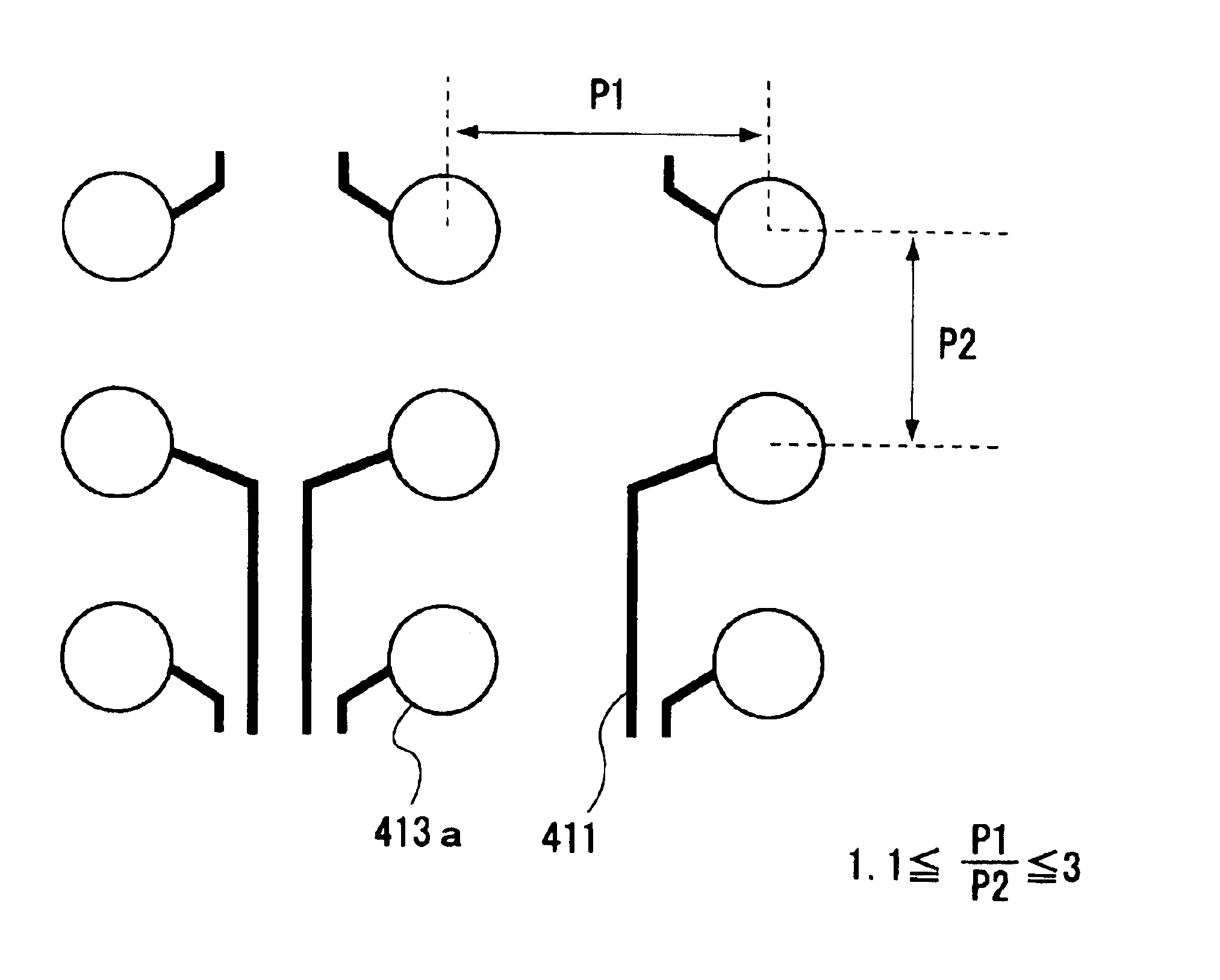
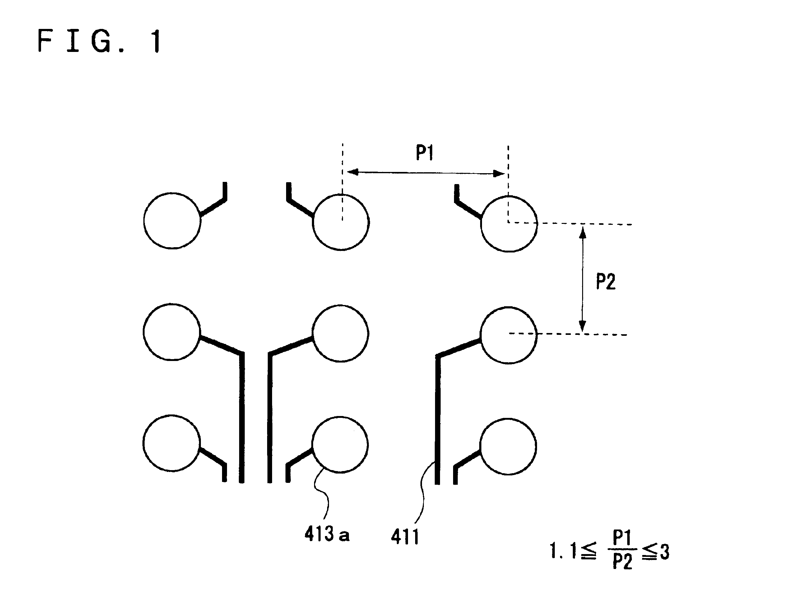
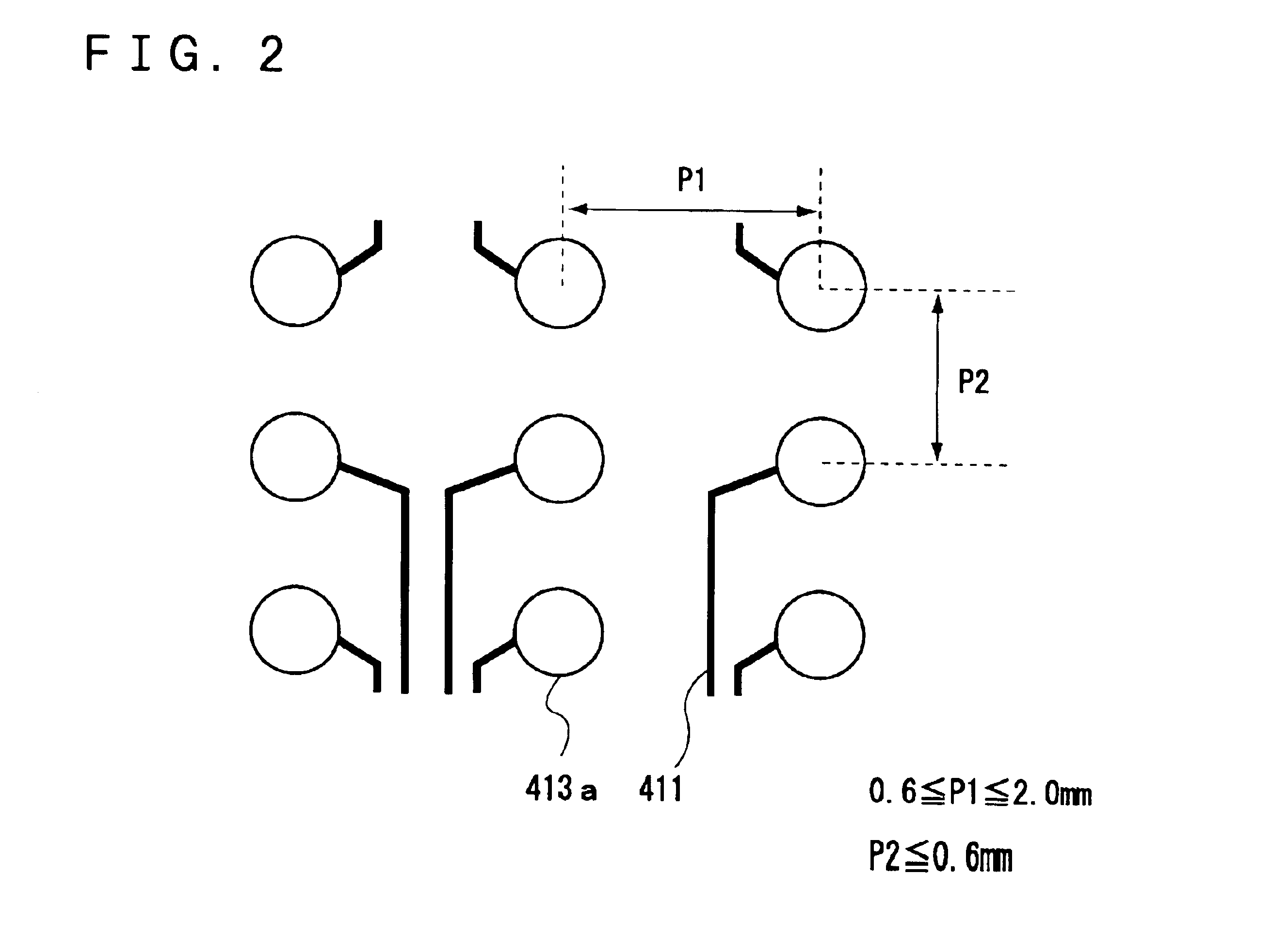
Referring to FIG. 1, a first embodiment is a circuit board including a plurality of pads 413a for mounting a semiconductor device with bumps and a plurality of wires 411 drawn from the plurality of pads 413a, the circuit board including a region where the pitch in the longitudinal direction and the lateral direction of the pads 413a are different, and the wires 411 being preferentially drawn from a wider pitch side of the longitudinal direction or the lateral direction of the pads 413a.

1. Pad

(1) Anisotropy

1) Ratio of Pitches

It is preferable to set the ratio P1 / P2 within the range of 1.01 to 3 where P1 is a wider pitch of the pads and P2 is a narrower pitch.

This is because when the ratio P1 / P2 becomes less than 1.01, it may be difficult to draw the wires to the exterior and to route them. On the other hand, when the ratio P1 / P2 has exceeded 3, the number of pads that can be arranged in unit area may be excessively limited, or adversely it becomes difficult to route the wires.

Therefo...

second embodiment

Referring to FIG. 15, a second embodiment is a mounting structure for a semiconductor device with bumps, characterized in that a semiconductor device with bumps is mounted to a circuit board via a solder material applied on pads, the circuit board including a region where the pitch in the longitudinal direction and the lateral direction of the pads are different from each other, in which the wires of the pads are preferentially drawn from a wider pitch side of the longitudinal direction or the lateral direction.

Points similar to those of the first embodiment will be omitted as appropriate and characteristic points of the second embodiment will be described hereinafter with particular emphasis thereon.

1. Structure

(1) Basic Structure

A mounting structure 360 for the semiconductor device with bumps according to the second embodiment basically includes the semiconductor device (interposer) 63 with bumps, a circuit board 361, and a solder material 365, as shown in FIG. 15. Since the semic...

third embodiment

A third embodiment is an electro-optic device characterized by including a semiconductor device with bumps mounted on a circuit board having a region where the pitch in the longitudinal direction and the lateral direction of the pads are different from each other as a driving element or a power-supply element, in which the wires of the pads are preferentially drawn from a wider pitch side of the longitudinal direction or the lateral direction.

A liquid crystal panel that forms an electro-optic device shown in FIG. 21 will be described as an example.

Referring to FIG. 22, the schematic structure of a liquid crystal panel 200 in FIG. 21 will first be described. FIG. 22 schematically shows the state of the liquid crystal panel 200 of FIG. 21 before a semiconductor IC and a flexible wiring board are mounted thereon. In the drawing, the dimensions are adjusted for convenience in the drawing and select components are omitted as appropriate.

The liquid crystal panel 200 includes a color filte...


PUM


Abstract

The present invention provides a circuit board including a plurality of pads for mounting a semiconductor device with bumps and a plurality of wires drawn from the respective pads, a mounting structure for the semiconductor device with bumps, and an electro-optic device and an electronic device. The circuit board has a region where the pitch in the longitudinal direction and the lateral direction of the plurality of pads are different from each other and the wires are preferentially drawn from a wider pitch side of the longitudinal direction or the lateral directions of the pads.

Description

BACKGROUND OF THE INVENTION1. Technical Field of the InventionThe present invention relates to a circuit board, a mounting structure for a semiconductor device with bumps, an electro-optic device and an electronic device. More particularly, the present invention concerns a circuit board in which the mounting position is not displaced even when a semiconductor device with fine bumps such as a ball grid array (hereinafter, referred to as a BGA) is mounted by reflowing, a mounting structure for the semiconductor device with the bumps, an electro-optic device and an electronic device including such a circuit board.2. Related ArtA method of mounting a quad flat package (QFP) on a printed circuit board (PCB) has been widely performed as a mounting method adapted to the tendency of fine-pitch and multiple-pin lead terminals of a semiconductor. This is used in a state in which the QFP that is a flat package having a large number of gull-wing lead terminals on four sides of the package is mo...

Claims


Application Information

Patent Timeline
Patent Type & Authority Patents(United States)
IPC IPC(8): H05K3/34H05K1/11H05K3/28H05K1/18H01L23/12H01L23/48
CPCH05K1/111H05K3/3436H05K3/284H01L2924/15311H01L2224/48465H01L2224/48227H01L2224/48091H01L2924/3025H05K2201/09227H05K2201/09381H05K2201/10977H01L2924/00014H01L2924/00Y02P70/50H05K1/18
Inventor ASHIDA, TAKESHI
Owner BOE TECH GRP CO LTD
Why Eureka
Try Eureka