Level shift circuitry having delay boost

a level shift circuit and boost technology, applied in logic circuits, pulse automatic control, pulse techniques, etc., can solve the problems of pedestal and potentially false switch, unable to guarantee the operation of existing level shift circuitry under all conditions, and increasing the difficulty of interfacing newer ic devices with legacy systems, so as to reduce the delay caused by pmos to nmos contention and reduce the rise and fall times.

Inactive Publication Date: 2005-02-08
GLOBALFOUNDRIES US INC
View PDF13 Cites 13 Cited by
  • Summary
  • Abstract
  • Description
  • Claims
  • Application Information

AI Technical Summary

Benefits of technology

The present invention addresses the above-mentioned problems, as well as others, by providing a level shifter circuit that includes a boost circuit for reducing the delay caused by PMOS to NMOS contention. In a first aspect the invention provides a level shift circuit, comprising: a pair of shift PFETs; a helper PFET for each of the shift PFETs; a pair of boost circuits for decreasing the rise and fall times of the pair of shift PFETs; and a trigger circuit for controlling the boost circuits.
In a second aspect, the invention provides a level shift circuit, comprising: a first inverter having an NFET with source tied to ground and a PFET with source tied to a shifted voltage via a helper PFET, the NFET and PFET being coupled together to define a first inverter node that provides a first level shifted output signal, wherein the NFET and PFET receive a first input signal; a second inverter having an NFET with source tied to ground and a PFET with source tied to the shifted voltage via a helper PFET, the NFET and PFET being coupled together to define a second inverter node that provides a second level shifted output signal, wherein the NFET and PFET receive a second input signal at an opposite logic state of the first input signal; a first boost device coupled to the first inverter node, wherein the first boost device is coupled to the shifted voltage and receives the second level shifted output signal as a control input; and a second boost device coupled to the second inverter node, wherein the first boost device is coupled to the shifted voltage and receives the first level shifted output signal as a control input.
In a third aspect, the invention provides an integrated circuit chip, comprising: a level shift circuit for shifting a signal at a first voltage potential at an input node to a second voltage potential at an output node; a boost circuit, driven by the second voltage potential, for decreasing a transition time of the signal between the first and second voltage; and a trigger circuit, coupled to an input of the boost circuit, for turning off the boost circuit when the signal at the output node reaches a predetermined voltage level.

Problems solved by technology

As core voltages continue to fall, interfacing newer IC devices with legacy systems has become more and more challenging.
As core voltages drop, existing level shift circuitry cannot be guaranteed to operate under all conditions.
If the NMOS to PMOS area ratio is not enough, a pedestal and potentially a false switch will occur on the falling / rising edge of the output signal of the level shifter.
If the drive strength of the PMOS devices is decreased to minimize pedestaling, performance will be severely compromised.

Method used


Image

  • Level shift circuitry having delay boost
  • Level shift circuitry having delay boost
  • Level shift circuitry having delay boost

Examples


Embodiment Construction

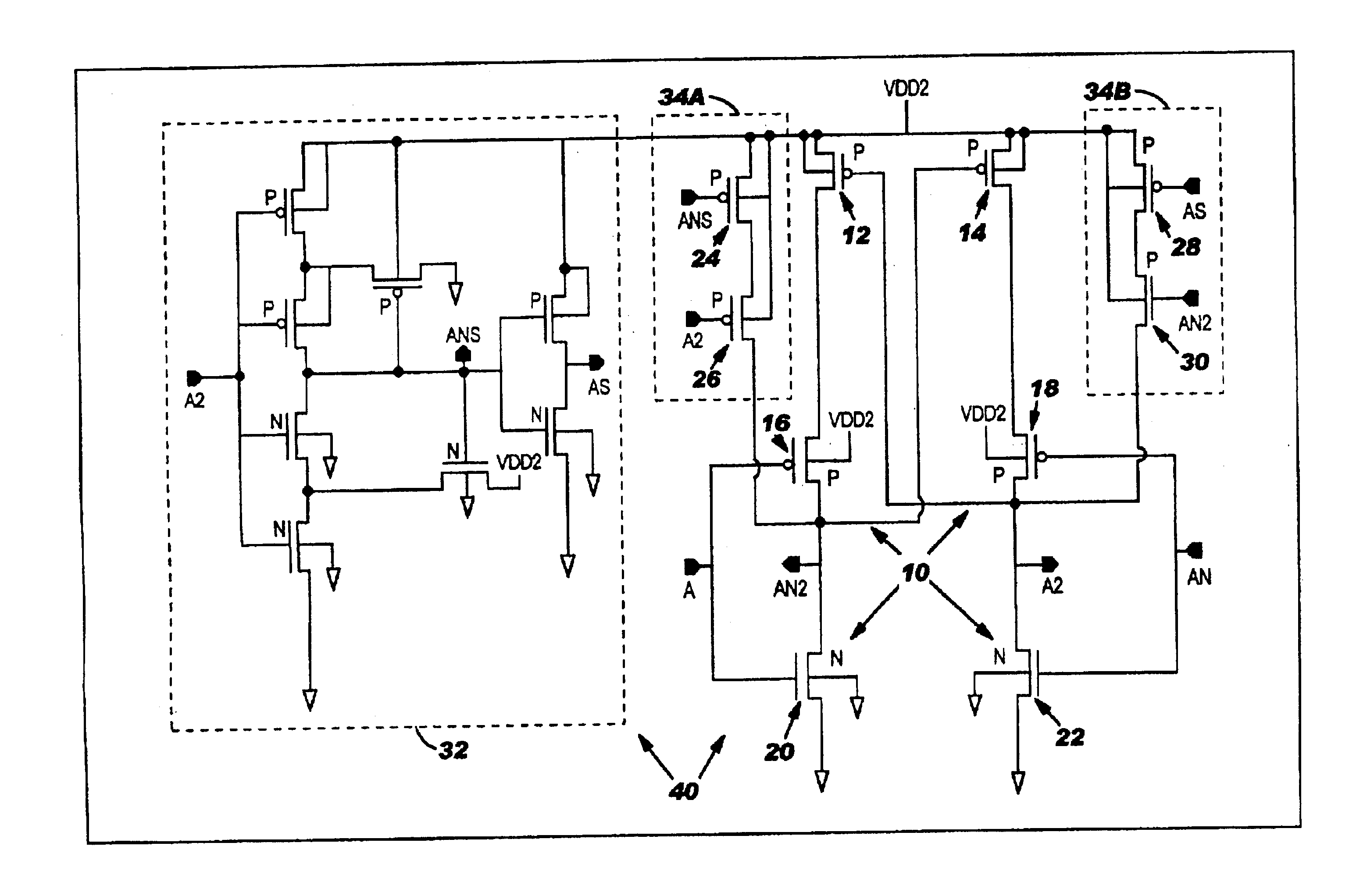
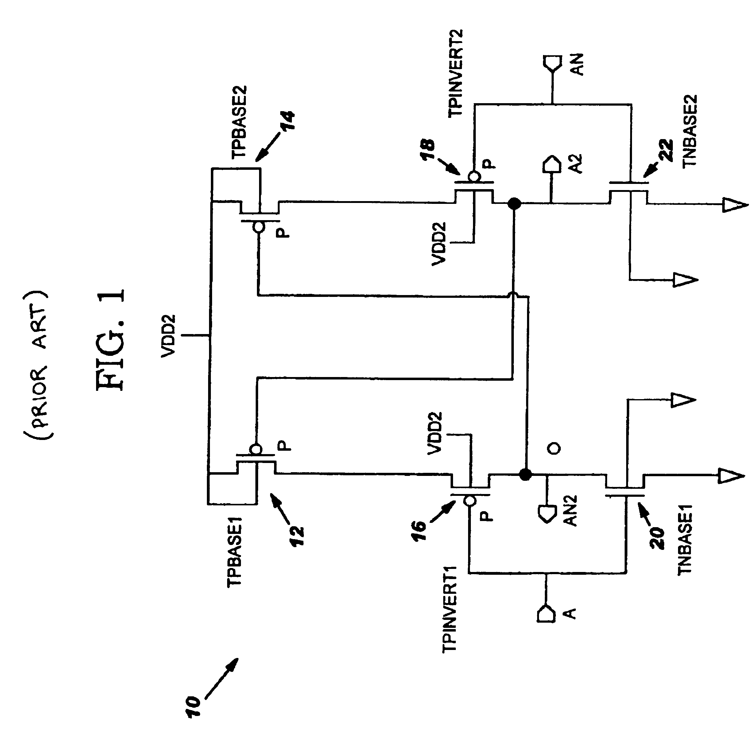
As shown in FIG. 3, the present invention provides a level shift circuit 40 that shifts voltages from a core voltage level VDD1 (not shown) to a second voltage level VDD2 such that the PMOS to NMOS contention is minimized without affecting performance. In an exemplary application, VDD1 may range from about 0.7-0.9 V and VDD2 may range from about 3.3-3.6 V. However, it should be understood that the level shift circuit 40 of the present invention is not limited to the above-mentioned voltage differences between VDD1 and VDD2, i.e., the invention can be implemented to handle voltage level shifts from 0.7 to 3.6V, or greater.

FIG. 3 depicts an exemplary device 11 having level shift circuit 40 in accordance with the present invention. Device 11 may comprise any type of integrated circuit device, chip, I / O device, etc., that requires a shifting of voltage levels. The level shift circuit 40 includes a level shifter 10 (as described in FIG. 1), boost circuitry 34A and 34B for decreasing the ...


PUM


Abstract

A level shift circuit that reduces PMOS to NMOS device contention whole decreasing output rise delays. The invention includes a device, comprising: a level shift circuit for shifting a signal at a first voltage at an input node to a second voltage at an output node; a boost circuit, driven by the second voltage, for decreasing a transition time of the signal between the first and second voltage; and a trigger circuit, coupled to an input of the boost circuit, for turning off the boost circuit when the signal at the output node reaches a predetermined voltage level.

Description

BACKGROUND OF INVENTION1. Technical FieldThe present invention relates generally to level shift circuitry, and relates more specifically to a level shifter having a voltage sensitive delay boost for enhancing the switching speed of the shift circuit.2. Related ArtAdvancements in integrated circuit (IC) technologies have allowed power supply voltages to decrease to very low levels. For instance, some chips implemented in 90 nm technologies can theoretically operate with core voltages as low as 0.9V, as compared to some legacy systems that operate at 3.3V. Traditionally, level shifter circuits, such as that shown in FIG. 1, have been utilized to shift a signal from a first core voltage level VDD1 (e.g., 0.9V) to a second voltage level VDD2 (e.g., 3.3V). As core voltages continue to fall, interfacing newer IC devices with legacy systems has become more and more challenging.In order to effectively shift between voltages, the level shifter circuit must be able to handle: (1) the differen...

Claims


Application Information

Patent Timeline
Patent Type & Authority Patents(United States)
IPC IPC(8): H03L5/00H03K3/012H03K3/356
CPCH03K3/012H03K3/356182H03K3/356113
Inventor BUCOSSI, WILLIAM L.
Owner GLOBALFOUNDRIES US INC
Why Eureka
Try Eureka