Pulse driven single bit line SRAM cell

a single bit line, sram cell technology, applied in the direction of information storage, static storage, digital storage, etc., can solve the problems of large arrays with difficult to meet timing constraints on word line and bit line, cell control voltage, etc., to reduce supply current and circuit noise, and reduce the physical space occupied by the memory cell

Inactive Publication Date: 2005-02-08
PICONETICS INTPROP TRUST
View PDF7 Cites 25 Cited by
  • Summary
  • Abstract
  • Description
  • Claims
  • Application Information

AI Technical Summary

Benefits of technology

One advantage of the present invention is that the write access transistor does not contend with the on-transistor of the second inverter during a write operation. This reduces supply current and circuit noise during a write operation.
Another advantage of the present invention is that the read access does not disturb the contents of the memory cell, because the output of the cell is buffered by a high-impedance gate input.
Yet another advantage of the present invention is that only a single bit line for a read or a write operation is needed, thereby reducing the physical space occupied by the memory cell.
Yet another advantage is that the memory cell does not require a variable positive supply voltage to power the cell, with one voltage for reading the cell and another voltage for writing the cell.
Yet another advantage is that the memory cell can be configured to accept either an active high or active low pulse as the write enable signal.

Problems solved by technology

One drawback of the circuit of FIG. 3 is that the cell control voltage must power an array of cells, but still be controllable.
Another drawback is that the timing constraints on the word line and bit line are difficult to meet for large arrays.

Method used


Image

  • Pulse driven single bit line SRAM cell
  • Pulse driven single bit line SRAM cell
  • Pulse driven single bit line SRAM cell

Examples


Embodiment Construction

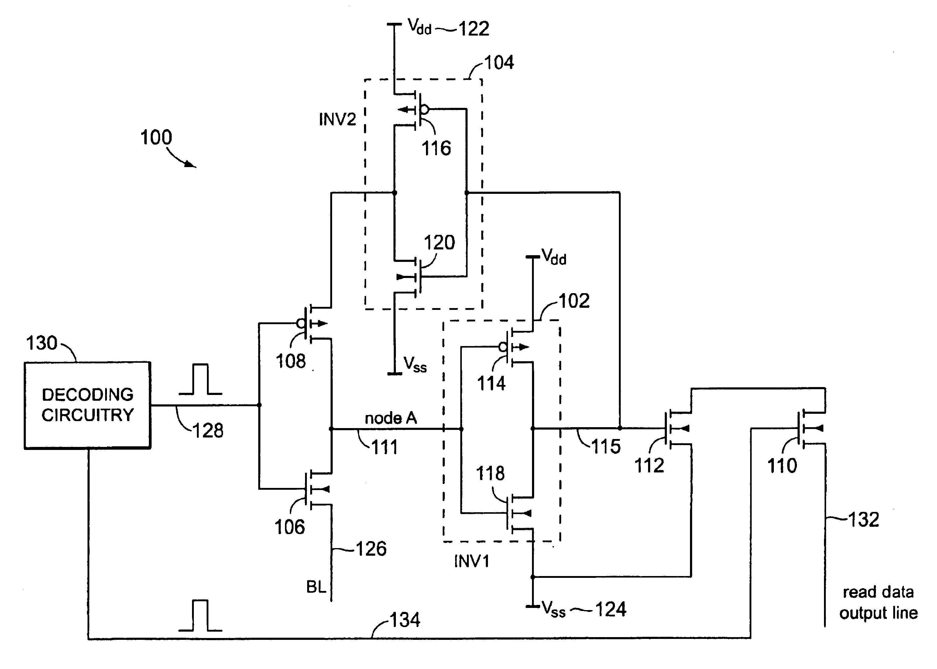
FIG. 4 shows a single bit line, pulse driven, static memory cell 100, in accordance with one embodiment of the present invention. The memory cell includes two inverters 102, 104, a write access transistor 106, a feedback-control transistor 108, a read-access transistor 110 and a read buffer transistor 112.

The two inverters 102, 104 each include a p-channel pull-up transistor 114, 116 and an n-channel pull-down transistor 118, 120 (with the respective gates and drains of the pull-up and pull-down transistors each tied together). The inverters 102, 104 operate between the positive voltage supply Vdd 122 and a return potential Vss 124. The first inverter 102 has an output 115 connected to the input of the second inverter 104 and the second inverter 104 has an output connected to the input of the first inverter 102 through the channel of the feedback-control transistor 108. Thus, the inverters 102, 104 are only cross-coupled when the feedback-control transistor 108 has a conductive chan...


PUM


Abstract

A single bit line, pulse-operated memory cell. The memory cell includes a first and second inverter, write access and feedback-control transistors, and read access transistor and read buffer transistors. The output of the first inverter is connected to the input of the second inverter and the output of the second inverter is connected to the input of the first inverter through the channel of the feedback-control transistor. The write access and feedback-control transistors are opposite types, and their gates are connected together so that when the feedback control transistor is on the write-access transistor is off and visa versa. Writing the cell thus avoids contending the with the on-transistor of the second inverter. The output of the cell is sensed by the gate of the buffer transistor and coupling the output of the buffer transistor through the read access transistor to the read output line.

Description

FIELD OF THE INVENTIONThis invention relates generally to a SRAM cell having a single bit line and more particularly to an SRAM cell configured to operate in response to a pulse-driven word line.DESCRIPTION OF THE RELATED ARTFIG. 1 show a prior art six-transistor static memory (SRAM) cell 10. The SRAM cell 10 includes two CMOS inverters 12, 14 that are cross-coupled (the output of each inverter is connected to the input of the other) to create a latch, and two access transistors16, 18 by which the latch is read or altered (written). The first inverter 12 includes PMOS transistor 20 and NMOS transistor 22. The second inverter 14 includes PMOS transistor 24 and NMOS transistor 26. The first access transistor 16 provides a channel between the output of the first inverter 12 and a first bit line 28, BL. The second access transistor 18 provides a channel between the output of the second inverter 14 and a second bit line 30, BLbar, which is the complement to the first bit line 28. The gat...

Claims


Application Information

Patent Timeline
Patent Type & Authority Patents(United States)
IPC IPC(8): G11C7/06G11C11/412
CPCG11C11/412G11C7/067
Inventor ZHANG, WEICHEN, FENGWU, JIANBIN
Owner PICONETICS INTPROP TRUST
Why Eureka
Try Eureka