Magnetic memory device implementing read operation tolerant to bitline clamp voltage (VREF)

a magnetic memory and bitline clamping technology, applied in the field of magnetic random access memory, can solve problems such as unstable read operation of magnetic memory cells, and achieve the effect of stable read operation

Active Publication Date: 2005-02-08
SAMSUNG ELECTRONICS CO LTD
View PDF5 Cites 18 Cited by
  • Summary
  • Abstract
  • Description
  • Claims
  • Application Information

AI Technical Summary

Benefits of technology

The present invention provides an MRAM, which is able to perform a stable rea

Problems solved by technology

As a result, a read operation of the

Method used


Image

  • Magnetic memory device implementing read operation tolerant to bitline clamp voltage (VREF)
  • Magnetic memory device implementing read operation tolerant to bitline clamp voltage (VREF)
  • Magnetic memory device implementing read operation tolerant to bitline clamp voltage (VREF)

Examples


first embodiment

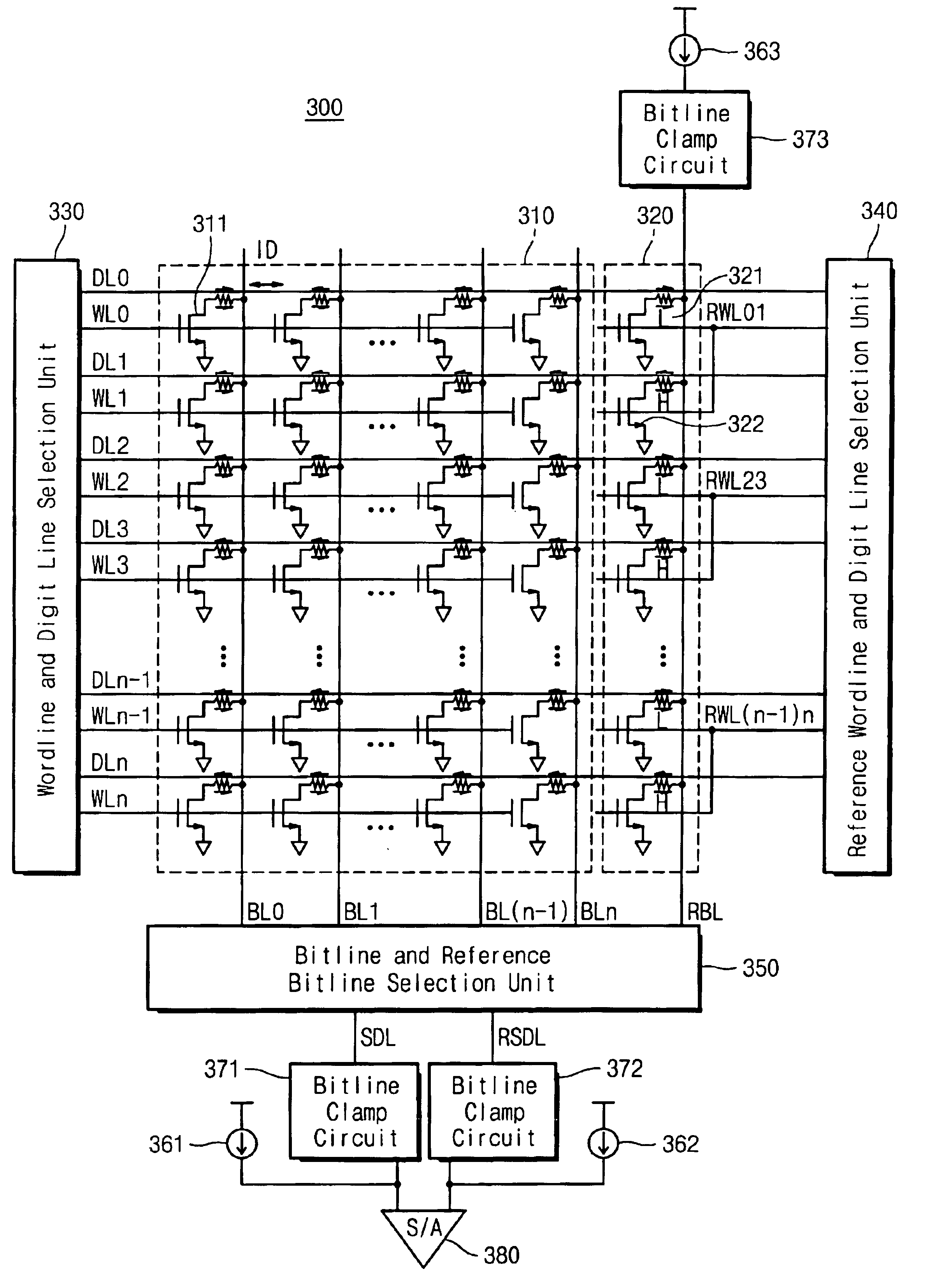
An MRAM according to the present invention will now be described with reference to FIG. 3.

Referring to FIG. 3, an MRAM 310 includes a memory array block 310, a reference memory array block 320, a wordline and digit line selection unit 330, a reference wordline and digit line selection unit 340, a bitline and a reference bitline selection unit 350, reference current supply units 361, 362, and 363, bitline clamp circuits 371, 372, and 373, and a sense amplifier (S / A) 380. The memory array block 310 has magnetic memory cells arranged at intersections of wordlines WL0, WL1, . . . , WLn−1, WLn (referred to in totality as WL), bitlines BL0, BL1, . . . , BLn−1, BLn (referred to in totality as BL), and digit lines DL0, DL1, . . . , and DLn−1, and DLn (referred to in totality as DL). The reference memory array block 320 has magnetic memory cells arranged at intersections of reference wordlines RWL01, RWL23, . . . , RWL(n−1)n (referred to in totality as RWL), a reference bitline RBL, and the ...

second embodiment

An MRAM according to the present invention will now be described with reference to FIG. 5.

Referring to FIG. 5, an MRAM 500 is substantially identical to the MRAM 300 of FIG. 3, except that a reference memory cell array block 520 is different from the reference memory cell array block 320 of FIG. 3. Elements of FIG. 5 that are the same in FIG. 3 will not be described in further detail. Referring to FIG. 5, the reference memory cell array block 520 has magnetic memory cells disposed at intersections of wordlines WL, digit lines DL, and a reference bitline RBL. Two magnetic cells 521 and 522, coupled to one wordline WL and one digit line DL, are coupled to the reference wordline RBL. Low level “L” data is stored in one magnetic memory cell 521, and high level “H” data is stored in the other magnetic memory cell 522.

A read operation of magnetic memory cell data in the MRAM 500 of FIG. 5 will now be described with reference to FIG. 6.

Referring to FIG. 6, in a case that data of the select...


PUM


Abstract

A magnetic memory device includes a memory cell array block and a reference memory cell array block having a plurality of magnetic memory cells arranged, respectively, at intersections of wordlines, digit lines, and bitlines, and reference wordlines, the digit lines, and a reference bitline, a first bitline clamp circuit coupled to a bitline to which a first selected magnetic memory cell is connected and supplying a first current to the first selected magnetic memory cell through the bitline, second and third bitline clamp circuits coupled to respective upper and lower ends of the reference bitline, for supplying a second current to selected magnetic memory cells in the reference memory cell array block through the reference bitline, and a sense amplifier for sensing and amplifying currents on first and second data lines, respectively connected to the bitline and the reference bitline, to judge data of the first selected magnetic memory cell.

Description

BACKGROUND OF THE INVENTION1. Field of the InventionThe present invention relates to a magnetic random access memory. More particularly, the present invention relates to a magnetic random access memory where a current of (I(H)+I(L)) / 2 flows to a reference cell irrespective of a bitline clamp voltage.2. Description of the Related ArtMagnetic random access memory (MRAM) is a kind of a non-volatile memory device including a plurality of magnetic memory cells. The MRAM utilizes a magnetoresistive effect occurring between a magnetic layer and an amagnetic layer, which constitute a multiple layer (bi-layer). When magnetization directions in the magnetic layer are identical to each other (parallel state), the magnetic resistance of a magnetic memory cell is minimal. When magnetization directions in the magnetic layer are opposite to each other (anti-parallel state), the magnetic resistance of a magnetic memory cell is maximal. The parallel state is called a logic low (“L”) state, and the a...

Claims


Application Information

Patent Timeline
IPC IPC(8): G11C7/12G11C7/00G11C11/15H01L43/08
CPCG11C7/12G11C11/1673G11C11/15
Inventor OH, HYUNG-ROKKIM, SU-YEONCHO, WOO-YEONG
Owner SAMSUNG ELECTRONICS CO LTD
Why Eureka
Try Eureka