Compact layout for a semiconductor device

a semiconductor device and compact technology, applied in semiconductor devices, semiconductor/solid-state device details, electrical apparatus, etc., can solve the problems of affecting the quality of heat conduction in the device, serious affecting the maximum achievable performance of the amplifier, etc., to achieve compact use, reduce inductance, and high-performance rf power amplification

Inactive Publication Date: 2005-02-15
SKYWORKS SOLUTIONS INC
View PDF4 Cites 8 Cited by
  • Summary
  • Abstract
  • Description
  • Claims
  • Application Information

AI Technical Summary

Benefits of technology

This invention is based on the observation that a semiconductor device comprising a set of one or more transistor elements over a substrate with a via hole therein may be made more compact if the set of transistor element(s) compactly surrounds the via hole. Preferably, the set of transistor element(s) also compactly surrounds an electrode to which the element(s) is electrically connected through at least one contact. In this manner, no extensive electrical interconnections need to be made between the via hole and the set of element(s), or between the electrode and the element(s). Compactly surrounding the electrode or the via hole means that the set surrounds the electrode or the via hole at an angle of at least 180 degrees.
Another aspect of the invention is based on the recognition that where a set of one or more transistor element(s) compactly surrounds an electrode to which the set is electrically connected, and where at least one of the element(s) is a bipolar junction transistor with a total emitter area not less than about 400 square microns, or an aggregate emitter length not less than about 10 microns, or both, the resulting semiconductor structure is able to amplify power with improved high performance.
Still another aspect of the invention is based on the recognition that high performance RF power amplification may be achieved by providing a semiconductor device comprising a set of one more transistor element(s) that compactly surrounds an electrode to which the set is electrically connected, and supplying a RF signal to the device, so that the device provides an amplified RF output signal.
The above aspects of the invention, taken either alone or in combination, provides one or more of the following advantages: compact use of space over the surface of the semiconductor substrate, reduced inductance, reduced DC voltage drop and improved heat conduction and heat dissipation properties.

Problems solved by technology

However, even when differences between elements of a power amplifier are minimized, layout and device geometries may seriously affect the maximum achievable performance of the amplifier.
Additionally these paths also affect the quality of heat conduction in the device.

Method used


Image

  • Compact layout for a semiconductor device
  • Compact layout for a semiconductor device
  • Compact layout for a semiconductor device

Examples


Embodiment Construction

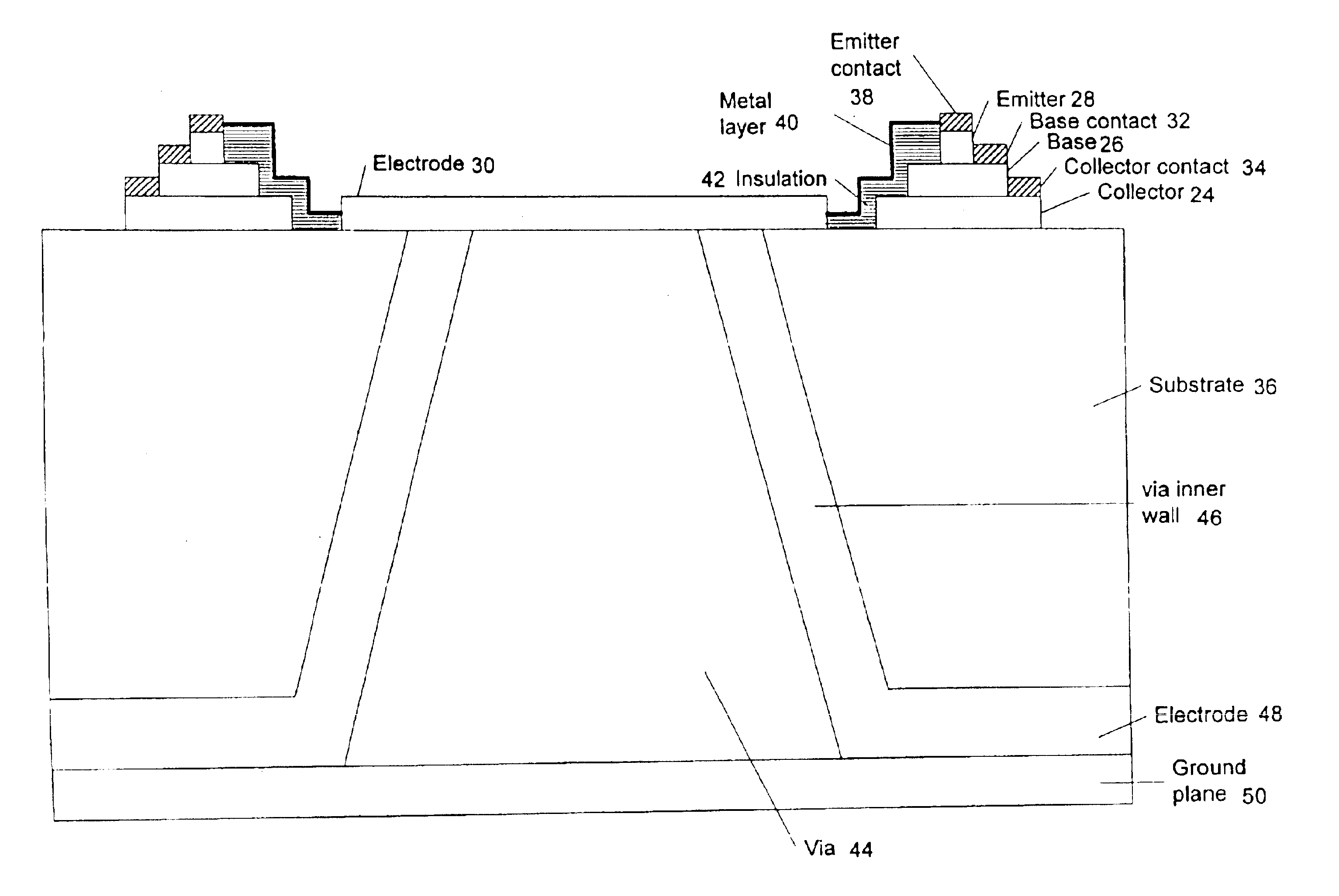
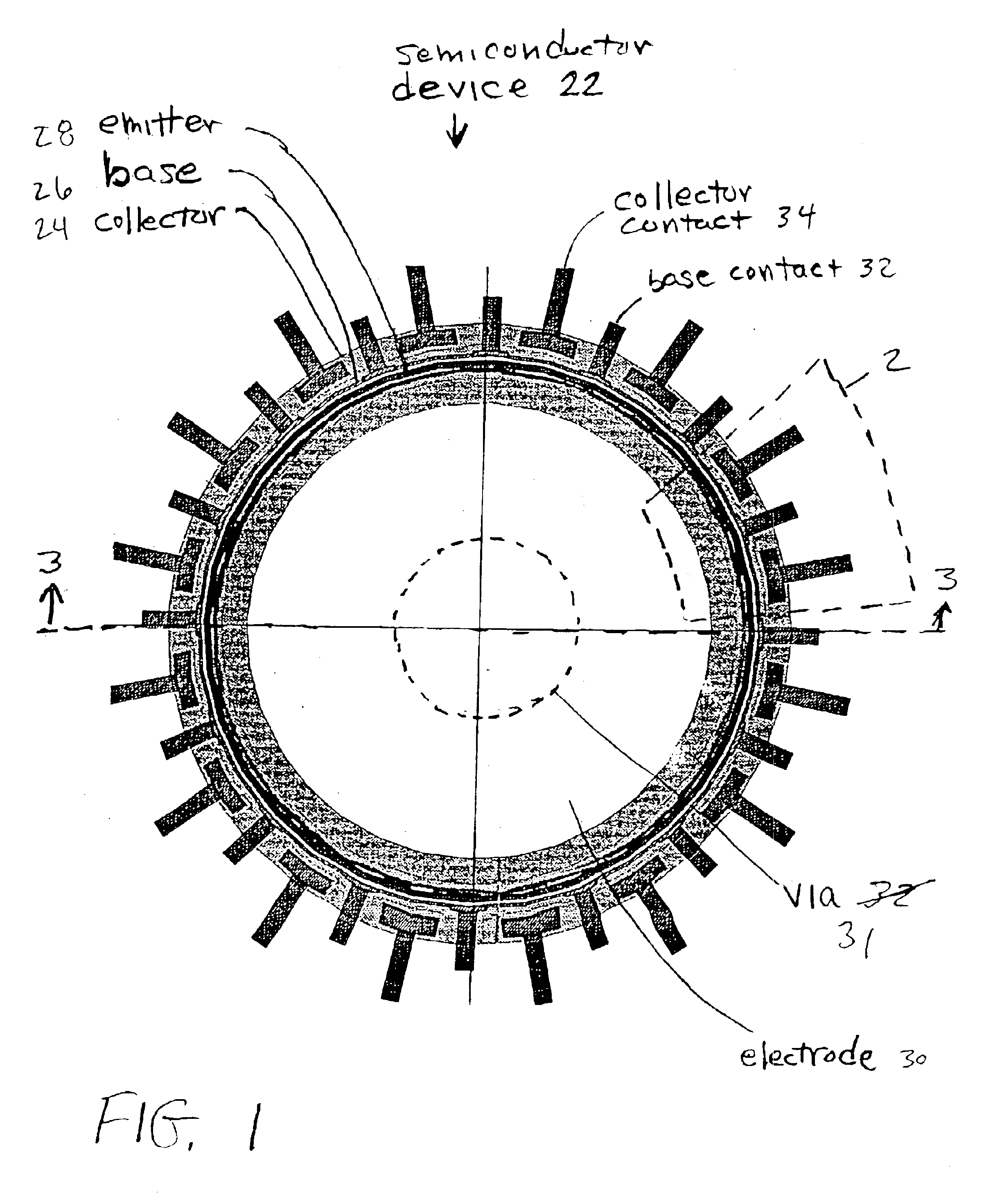
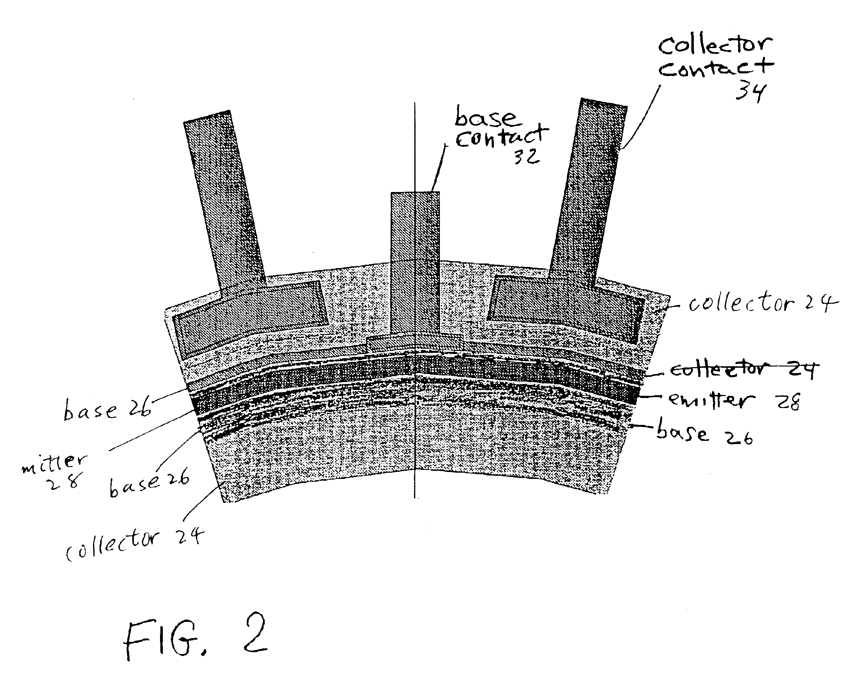
A preferred embodiment of the present invention is shown in FIG. 1. FIG. 1 shows a top view of a GaAs semiconductor device 22 with a circular layout. While device 22 may be constructed using GaAs, it will be understood that it may also be constructed using other types of semiconductor material such as silicon. On a substrate upper surface, a continuous transistor element surrounds a circular layout and includes transistor layers for a collector 24, a base 26 and an emitter 28. An electrode 30 lies above a via 31 in the substrate. A section of the device is shown in FIG. 2. Base contacts 32 connect to the base 26, and collector contacts 34 connect to the collector 24. Although not shown in FIGS. 1 and 2, a metal connection joins the emitter 28 and the electrode 30.

FIG. 3 shows a cross-sectional view of the device. The collector 24 is disposed on the upper surface of the substrate 36 in the shape of a mesa. Similarly the base 26 is disposed in the shape of a mesa on top of the collect...


PUM


Abstract

A semiconductor device includes a semiconductor substrate, an electrode disposed on an upper surface of the substrate, and a set of one or more transistor element(s) disposed on the upper surface of the substrate. The set of transistor element(s) compactly surrounds the electrode with a threshold distance. In one embodiment, the set also compactly surrounds a via hole. In another, the element(s) comprises a bipolar junction transistor that has an aggregate emitter length of not less than 10 microns. In still another embodiment, the device is coupled to a RF circuit for power amplification.

Description

BACKGROUND OF THE INVENTION1. Field of InventionThe present invention relates to semiconductor devices and more particularly to a compact layout for a semiconductor device.2. Description of Related ArtTypically in the design of a power amplifier, a number of transistor elements are arranged in rows and columns and then connected to provide a large equivalent power device. For example, FIG. 11 shows a conventional layout design for a semiconductor device 132 where a number of BJTs (Bipolar Junction Transistors) 134 are arranged in rows on the upper surface of a semiconductor substrate. Each BJT 134 includes an emitter contact 136, a base contact 138, and a collector contact 140. The emitter contacts 136 are connected by metal 142 to an electrode 144 that lies between the rows of BJTs 134, and the electrode 144 lies above vias 146 that provide an electrical connection to ground. The use of vias for electrical connections is well known in the art of semiconductor devices. (“Semiconduct...

Claims


Application Information

Patent Timeline
Patent Type & Authority Patents(United States)
IPC IPC(8): H01L29/66H01L29/732H01L23/48H01L29/02H01L23/482H01L29/06
CPCH01L23/4824H01L29/0657H01L29/0692H01L29/732H01L2924/0002H01L2924/00
Inventor KIAEI, ALISOLTAN, MEHDI FREDERICKRAJAEI, ALIRATEGH, HAMID REZA
Owner SKYWORKS SOLUTIONS INC
Why Eureka
Try Eureka