Semiconductor device testing apparatus and a test tray for use in the testing apparatus

a testing apparatus and semiconductor technology, applied in the direction of individual semiconductor device testing, semiconductor/solid-state device testing/measurement, instruments, etc., can solve the problems of poor utilization ratio of expensive ic testers, and limited number of ic sockets, so as to reduce the time required for complete testing and enhance the utilization ratio

Inactive Publication Date: 2005-02-15
ADVANTEST CORP
View PDF12 Cites 21 Cited by
  • Summary
  • Abstract
  • Description
  • Claims
  • Application Information

AI Technical Summary

Benefits of technology

A first object of the present invention is to provide an IC tester which is capable of reducing the time required to complete testing on all of the ICs to thereby enhance the utilization ratio.
A second object of the present invention is to provide an IC tester which is capable of transporting test trays from the soak chamber through the testing section to the exit chamber and which provides an enhanced simultaneous measurement throughput in number of ICs.
A third object of the present invention is to provide an IC tester which provides an increased throughput in number of ICs through the loader and unloader sections to thereby shorten the time required to complete testing on all of the ICs to be tested.
A fourth object of the present invention is to provide a test tray for use in an IC tester which provides for transporting test trays from the soak chamber through the testing section to the exit chamber in an efficient manner.

Problems solved by technology

This, however, requires a very long time to go through the test on all of the ICs, leading to a poor utilization ratio of the expensive IC tester and hence the serious disadvantage that the testing cost per IC is greatly increased.
However, there is a limit to the number of IC sockets which can be mounted on a tester head, which in turn imposes a limit on the increase in simultaneous measurement throughput in number of ICs.
In contrast, in the case that the testing time in the testing section 42 is relatively short, failure to transport test trays to the testing section 42 at high speed would involve a longer lost time in the testing operation in the testing section 42, resulting in undesirably prolonging the working time of the IC tester.
However, although it would not take much cost to make the speed of operation of the test tray transporting mechanism of only limited extent, it would require substantial cost to increase the operation speed to nearly the maximal limit, providing the disadvantage of rendering the initial cost of the entire IC tester very expensive.
Not only is it costly to increase the throughput in number of ICs, but also there is naturally a limit to increasing the throughput in number of ICs.

Method used


Image

  • Semiconductor device testing apparatus and a test tray for use in the testing apparatus
  • Semiconductor device testing apparatus and a test tray for use in the testing apparatus
  • Semiconductor device testing apparatus and a test tray for use in the testing apparatus

Examples


sixth embodiment

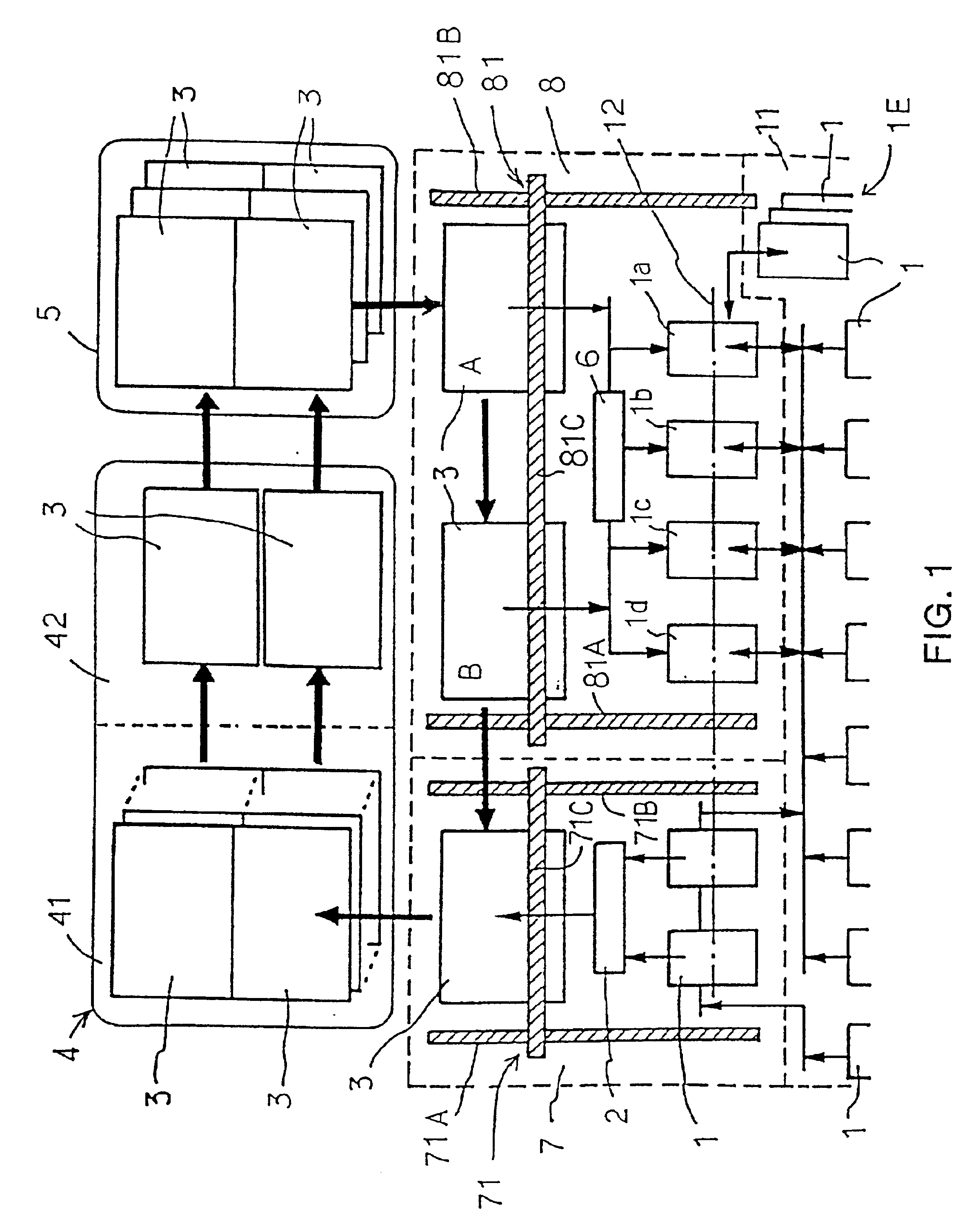
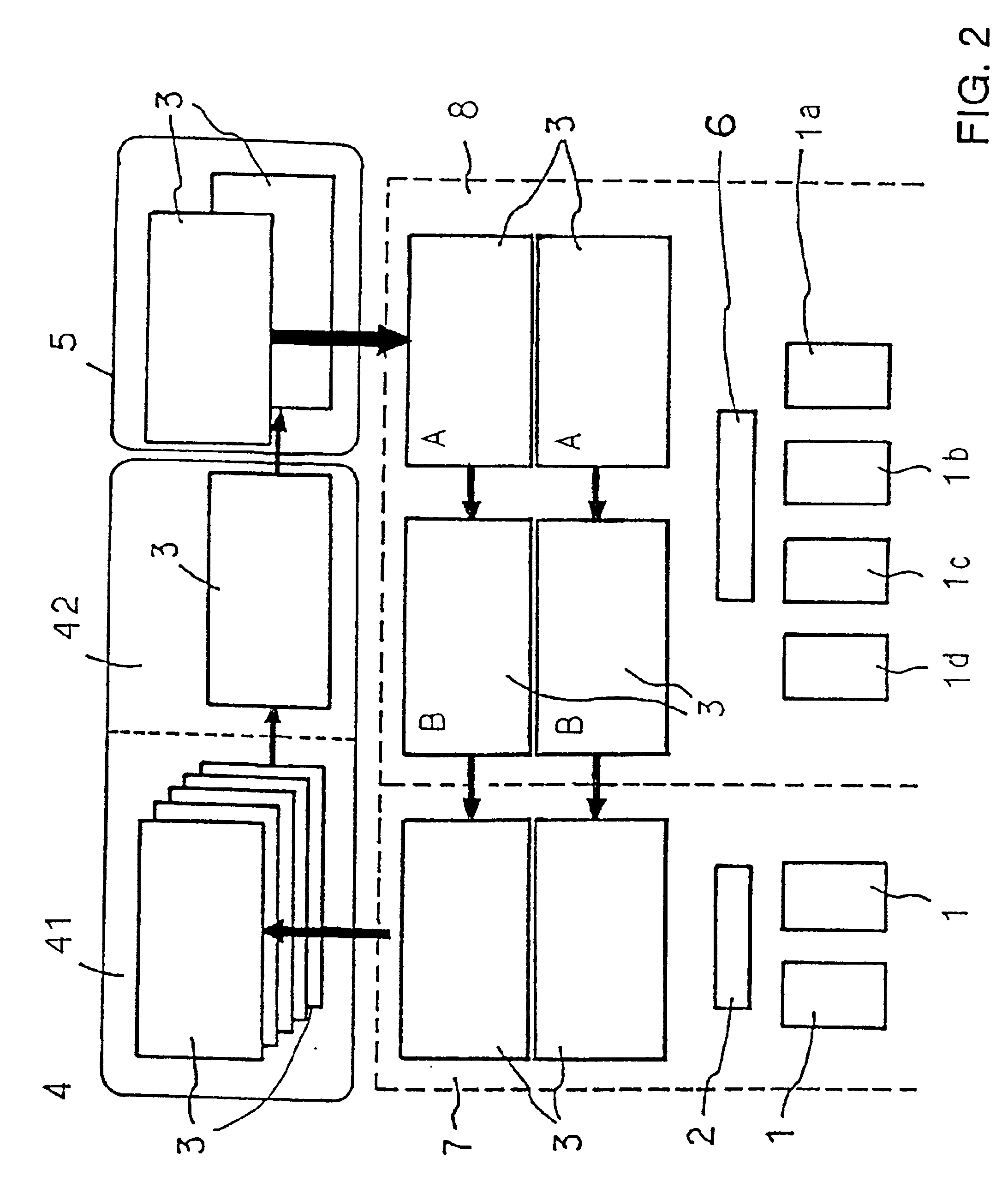
FIGS. 9 and 10 are a schematic perspective view and a side view, with the constant temperature chamber in cross-section, respectively illustrating the construction according to the present invention.

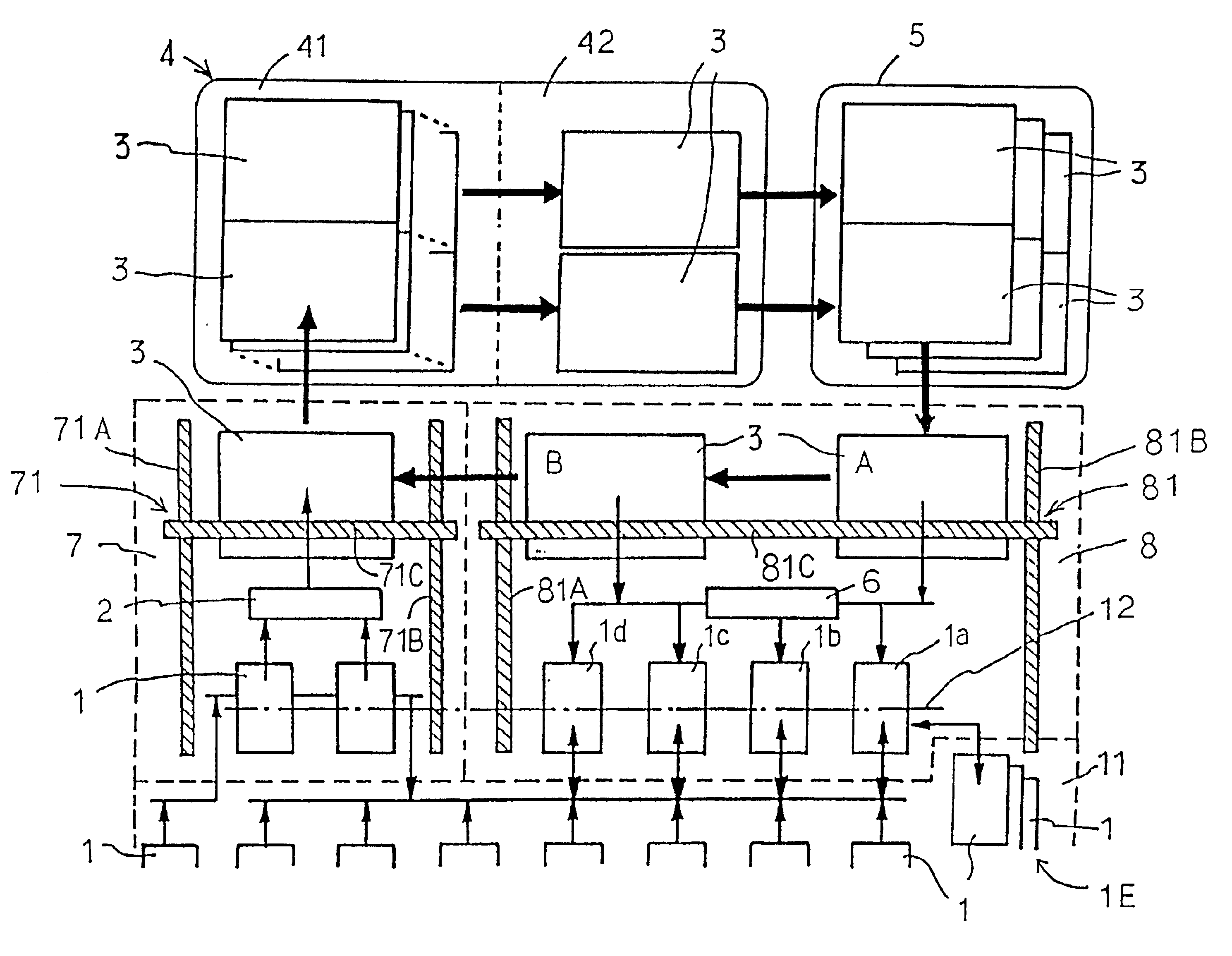
The IC tester of this sixth embodiment is configured such that a constant temperature chamber 4 is equipped with a vertical transport mechanism in the interior thereof which constitutes a soak chamber 41, the top of the constant temperature chamber 4 (at the elevation of the uppermost stage of the vertical transport mechanism) comprising a testing section 42 with a tester head 9 being mounted facedown in the top wall of the constant temperature chamber 4 while an loader section 7 and an unloader section 8 are integrated together and equipped with a common vertical transport mechanism.

In this embodiment, each stage of the vertical transport mechanism for supporting test trays thereon in the constant temperature chamber 4 has a lateral width approximately equal to the length of the major e...


PUM


Abstract

An IC tester which is capable of reducing the time required before completion of testing on all of ICs to be tested is provided. The depth (length in the Y-axis direction) of the constant temperature chamber 4 and the exit chamber 5 is expanded by a dimension corresponding approximately to one transverse width (length of the minor edge) of the rectangular test tray 3, and two generally parallel test tray transport paths or alternatively a widened test tray transport path broad enough to transport two test trays simultaneously with the two test trays juxtaposed in a direction transverse to the widened test tray transport path are provided in the section of test tray transport path extending from the soak chamber 41 in the constant temperature chamber 4 through the testing section 42 in the constant temperature chamber 4 to the exit chamber 5 so that two test trays may be simultaneously transported along the two test tray transport paths or the widened test tray transport path.

Description

TECHNICAL FIELDThe present invention relates to a semiconductor device testing apparatus suitable for testing semiconductor integrated circuit elements which are typical of semiconductor devices, and more particularly to a semiconductor device testing apparatus of the type in which semiconductor devices are transported to a testing section or test section where they are tested for their electrical characteristics, followed by being carried out of the test section and then being sorted out into conforming articles and non-conforming articles on the basis of the test results, and to a test tray for use in the IC tester in which the tray is moved in a circulating manner along a predetermined path of transport.BACKGROUND ARTMany semiconductor device testing apparatuses (commonly called IC tester) for measuring the electrical characteristics of semiconductor devices to be tested (commonly called DUT (device under test)) by applying a signal of a predetermined test pattern to the devices ...

Claims


Application Information

Patent Timeline
Patent Type & Authority Patents(United States)
IPC IPC(8): G01R31/28G01R31/01
CPCG01R31/2893G01R31/2867G01R31/2851G01R31/01G01R31/26H01L22/00
Inventor ITO, AKIHIKOKOBAYASHI, YOSHIHITOMASUO, YOSHIYUKIYAMASHITA, TSUYOSHI
Owner ADVANTEST CORP
Why Eureka
Try Eureka