System and method for measuring a capacitance of a conductor

a technology of capacitance and conductor, applied in the field of measurement, can solve the problems of incompatibility with neighboring components, inability to meet the requirements of product specifications, and inability to meet the requirements of measurement, so as to achieve the elimination of capacitance, high-quality measurement, and elimination of the effect of capacitan

Inactive Publication Date: 2005-02-15
TEXAS INSTR INC
View PDF5 Cites 4 Cited by
  • Summary
  • Abstract
  • Description
  • Claims
  • Application Information

AI Technical Summary

Benefits of technology

Certain embodiments of the present invention may provide a number of technical advantages. For example, according to one embodiment of the present invention, a measurement approach is provided that measurement approach is provided that allows isolation and highly accurate measurement of the capacitance between a target conductor and one or more selected conductors in a structure. This is a result of the elimination of the capacitance between the target conductor and the non-selected conductors in the structure. The elimination of their capacitance is achieved by charging and discharging the target conductor and non-selected conductors in phase so that no charge difference occurs, effectively shorting these conductors. Accordingly, the capacitance of conductors that may otherwise act to negatively influence a capacitance measurement are removed from the measurement equation.
Another technical advantage of one embodiment of the present invention is a result of a null structure or a reference structure that is used to offset parasitic capacitances inherent in the measurement circuit. Measurement circuits may have parasitic capacitances stemming from transistors and other such components that generate an electric field and corresponding capacitance. In accordance with the teachings of the present invention, the null or reference structure operates to compensate for or offset the parasitic capacitances in the capacitance measurement.
Yet another technical advantage of one embodiment of the present invention is a result of the charging and discharging of conductors coupled to the measurement circuit. This allows the steady state current on the drain of an associated p-element to be obtained in order to determine a capacitance therefrom. Thus, an alternating current (AC) phenomenon may be converted into a direct current (DC) value, capable of a more simplistic, accurate, and direct measurement. Embodiments of the present invention may enjoy some, all, or none of these advantages. Other technical advantages may be readily apparent to one skilled in the art from the following figures, description, and claims.

Problems solved by technology

Errors in modeling of the capacitance of semiconductors may contribute to discrepancies between the actual performance and reliability of integrated circuits when manufactured as compared with that predicted by design simulations.
This may result in reduced tolerances in product specifications, incompatibility with neighboring components, poor performance, or the non-operation of associated devices.
Several approaches for measuring system parameters (such as capacitance, for example) that have been employed are not satisfactory in all respects.
For example, many of these approaches involve testing structures that are too large or cumbersome to accurately identify a capacitance associated with the device or structure under test.
Additionally, hand measurements are virtually impossible and do not provide a feasible alternative for measuring capacitances associated with complex circuitry.
In addition, many of these approaches involve measuring components or elements that inadvertently interact with the architecture targeted for the capacitance measurement.
Such environmental effects generally cause inaccurate capacitance values to be obtained for a target device and further complicate the measurement process.
Other approaches to measuring capacitances or other system parameters may be generally inadequate because they are destructive in nature, potentially sacrificing valuable product segments in order to initiate the measuring or testing process.

Method used


Image

  • System and method for measuring a capacitance of a conductor
  • System and method for measuring a capacitance of a conductor
  • System and method for measuring a capacitance of a conductor

Examples


Embodiment Construction

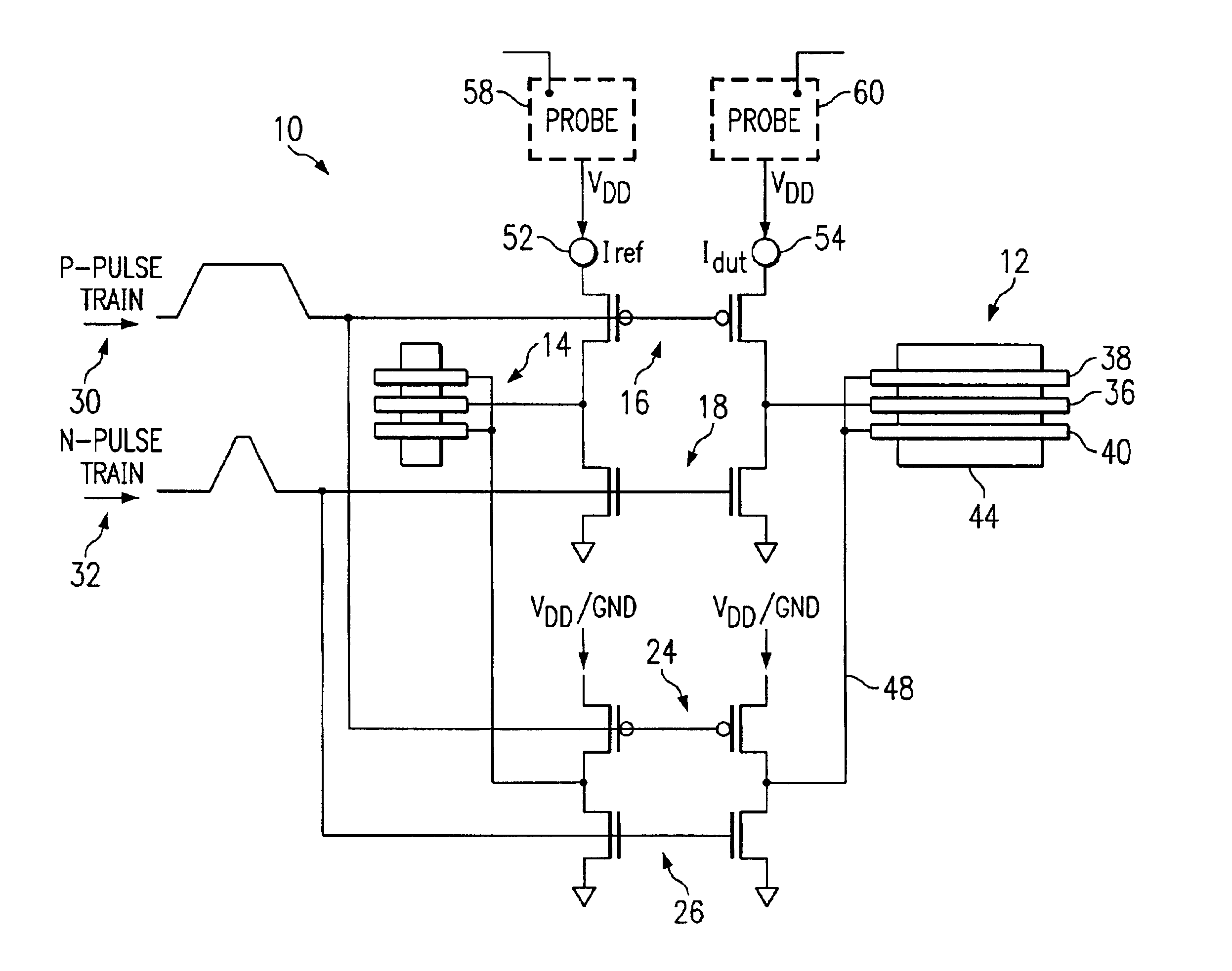
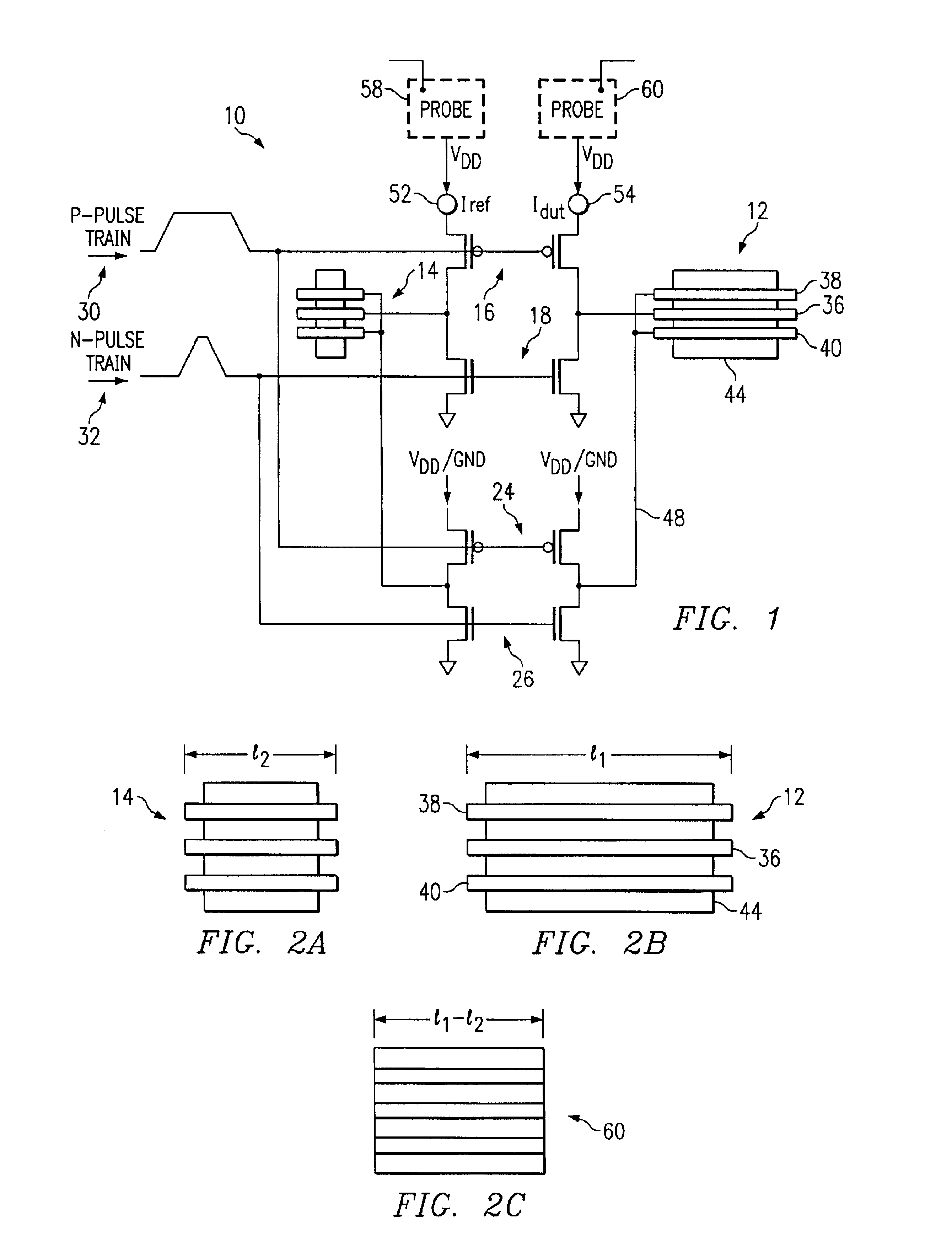
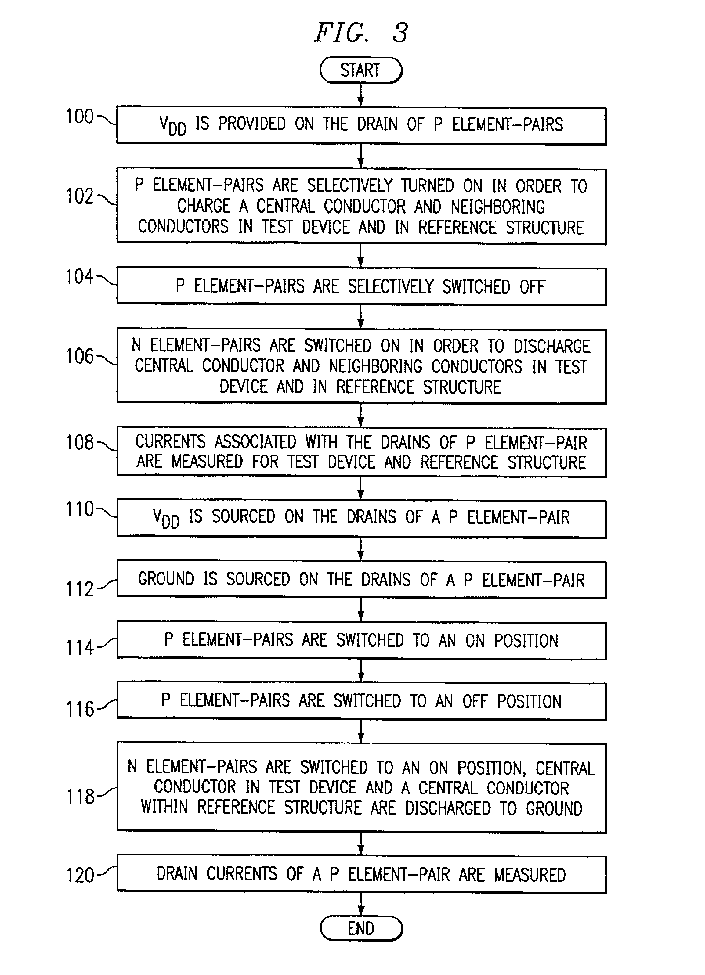
FIG. 1 is a simplified block diagram of a measurement system 10 for measuring a capacitance associated with a conductor, component or object. Measurement system 10 includes test device 12, a reference structure 14, a first set of p and n element-pairs 16 and 18, and a second set of p and n element-pairs indicated generally at 24 and 26. In general, each element or section within test device 12 may have an additional set of p and n element-pairs similar to those illustrated in FIG. 1. Measurement system 10 additionally includes a p-pulse train input indicated generally at 30 and an n-pulse train input indicated generally at 32. The pulse trains may be arranged such that when one selected p element is ON, the n element is OFF and when the p element is OFF, the n element is ON.

In accordance with the teachings of the present invention, measurement system 10 operates to measure a capacitance associated with an element or section within test device 12. Elements within test device 12 may b...


PUM


Abstract

A method for measuring a capacitance of a device under test is provided that includes selectively charging and discharging a first conductor with a first set of p and n element-pairs in response to a voltage potential applied to the first set of p and n element-pairs. The method further includes selectively charging and discharging a second conductor with a second set of p and n element-pairs in response to a voltage potential applied to the second set of p and n element-pairs. Currents are measured at drains associated with the first set of p element-pairs as the first and second conductors charge and discharge such that a capacitance associated with the first conductor may be determined that is based on the drain currents.

Description

TECHNICAL FIELD OF THE INVENTIONThis invention relates in general to the field of measurement and more particularly to a system and method for measuring a capacitance of a conductor.BACKGROUND OF THE INVENTIONAs integrated circuits have grown more complex, the ability to accurately measure the capacitance associated with semiconductor devices has equally grown more critical. Errors in modeling of the capacitance of semiconductors may contribute to discrepancies between the actual performance and reliability of integrated circuits when manufactured as compared with that predicted by design simulations. This may result in reduced tolerances in product specifications, incompatibility with neighboring components, poor performance, or the non-operation of associated devices. Accurate capacitance measurements for a given system provide the ability for correct specifications to be generated, whereby corresponding components or elements can function properly based on anticipated system para...

Claims


Application Information

Patent Timeline
Patent Type & Authority Patents(United States)
IPC IPC(8): G01R27/26G01R31/28G01R31/316
CPCG01R27/2605
Inventor MCNUTT, MICHAEL J.SARMA, ROBIN C.LIN, YU-SANG
Owner TEXAS INSTR INC
Why Eureka
Try Eureka