Device and method for reducing lag and blooming in amorphous silicon sensor arrays

a technology of amorphous silicon and image array, applied in the field of amorphous silicon image array, can solve the problems of ghost image that remains for several tens of seconds, increased diode capacitance and pixel noise, and image lag in full fill factor image arrays, etc., to achieve the effect of reducing lag and blooming

Inactive Publication Date: 2005-02-15
XEROX CORP
View PDF2 Cites 17 Cited by
  • Summary
  • Abstract
  • Description
  • Claims
  • Application Information

AI Technical Summary

Benefits of technology

According to another aspect of the present invention, a clamping circuit in a full fill factor sensor array is provided that reduces lag and blooming including a gate line, a data line, a bias plane carrying a bias voltage, a clamp line carrying a clamping voltage, a drain line carrying a drain voltage, a switching TFT having a source, a drain, and a gate, wherein the source or drain of the switching TFT is connected to the data line and the gate is connected to the gate line. The clamping circuit further includes a photodiode having an anode, a cathode, and a storage node, wherein the anode is connected to the other of the source or drain of the switching TFT and the cathode is connected to the bias plane. The clamping circuit further includes a clamp TFT having a source, a drain, and a gate, wherein the gate of the clamp TFT is connected to the clamp line, the source or drain of the clamp diode is connected to the storage node of the photodiode, and the other of the source or drain of the clamp TFT is connected to the drain line.

Problems solved by technology

This results in a ghost image that remains for several tens of seconds after the image was taken.
Thus, the benefit of reduced image lag provided by increasing the effective field across the diode must be weighed against the inevitable increase in sensor dark current and, in the case of thinner photodiodes, increased diode capacitance and increased pixel noise.
Full fill factor image arrays also suffer from image lag.
In addition to image lag, however, full fill factor image arrays also suffer blooming.
Conventional TFT full fill factor sensor arrays also lack a means for testing the TFT matrix prior to depositing the overlying collection electrode and sensor layer.
This solution, however, requires a capacitor at each pixel making it harder to form smaller pixels.
Another disadvantage is that the added capacitors add increased pixel noise to the electronic noise of the array.

Method used


Image

  • Device and method for reducing lag and blooming in amorphous silicon sensor arrays
  • Device and method for reducing lag and blooming in amorphous silicon sensor arrays
  • Device and method for reducing lag and blooming in amorphous silicon sensor arrays

Examples


Embodiment Construction

Reference will now be made in detail to the preferred embodiments of the invention, examples of which are illustrated in the accompanying drawings.

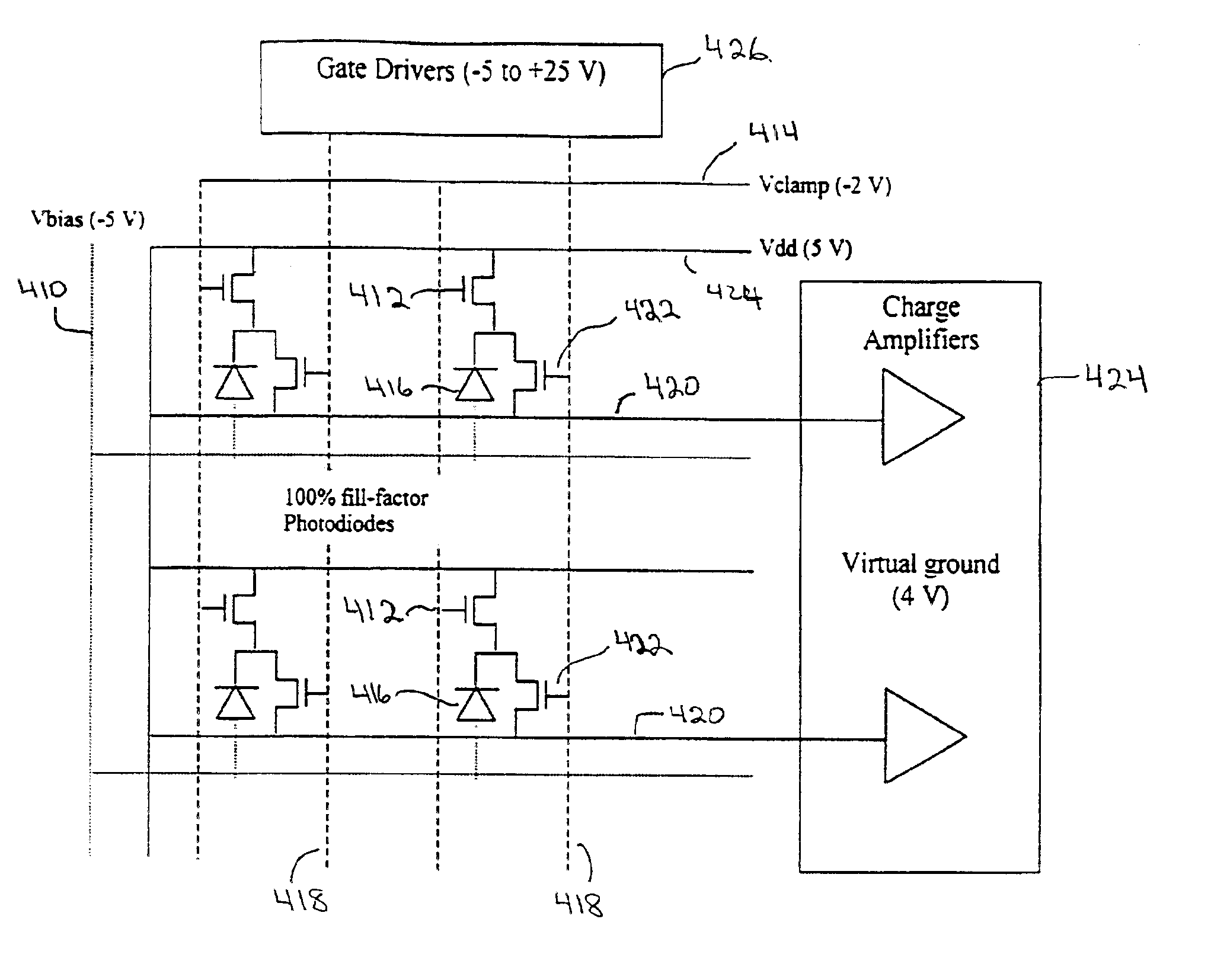
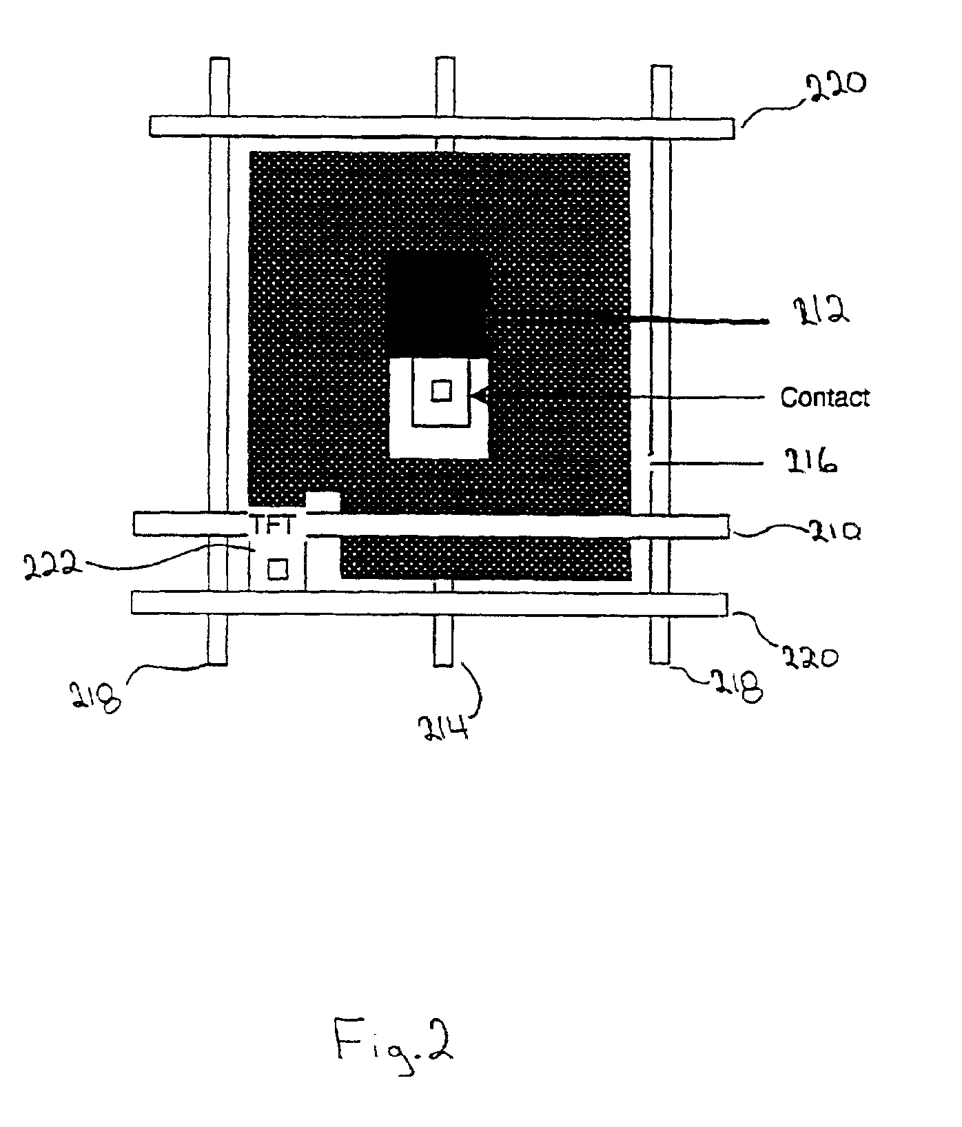
FIG. 2 shows a pixel layout of an image array including a clamping diode consistent with one embodiment of the invention. In addition to the conventional data lines 220, gate lines 218, TFT 222, and photodiode 216, the pixel of the invention includes a common bias line 210 and clamp line 214 running between each gate 218 and data line 220. It also includes a clamping diode 212 connected between the drain line and the pixel storage node.

The clamping diode 212 reduces image lag by preventing the voltage across the photodiode 216 from dropping below a specific threshold. Thus, even when the photodiode 216 is subject to illumination that would normally saturate the pixel, the photodiode remains under reverse bias.

FIG. 3 depicts the pixel circuit consistent with one embodiment of the present invention. The pixel circuit includes a gate line 31...


PUM


Abstract

A clamping circuit including a clamping diode, a bias line, and a clamp line is incorporated into a pixel circuit of amorphous silicon sensor arrays. The clamp diode in each pixel prevents the voltage across the photodiode from dropping below a specific threshold. By keeping the photodiode under reverse bias even under conditions that may otherwise saturate the pixel, image lag is reduced. In full fill factor amorphous silicon sensor arrays, a clamping circuit includes a clamp TFT, a bias plane, a clamp line, and a drain line. The clamp TFT reduces lag and blooming by draining off excess current developed under overexposure conditions. A method to globally reset a sensor array and a method to test and repair a TFT matrix in full fill factor sensor arrays without damaging the overlying collection electrode and sensor layer are also provided.

Description

FIELD OF THE INVENTIONThe present invention relates generally to amorphous silicon image arrays, and more particularly to amorphous silicon image arrays that reduce lag and blooming.BACKGROUND OF THE INVENTIONConventional amorphous silicon (a-Si) image arrays typically comprise an array of pixels and an associated matrix of rows and columns of address lines to electrically access each pixel. Each pixel has a photodiode and thin film transistor (TFT). The gate of each TFT is coupled to a scan line and the source (or alternatively the drain) of each TFT is coupled to a data line. These address lines are used to read the signal from respective pixel photodiodes.Image lag affects a-Si image sensors when a pixel is exposed to sufficient illumination to populate deep traps in the a-Si, which traps release charge long after the pixel has been exposed. The effect is greatly excerbated when a photodiode is exposed to sufficient intensity such that the voltage across the photodiode drops to z...

Claims


Application Information

Patent Timeline
Patent Type & Authority Patents(United States)
IPC IPC(8): H01L27/12H04N3/15H04N5/335H04N5/359H04N5/369
CPCH01L27/12H04N5/335H04N3/1568H04N25/626
Inventor WEISFIELD, RICHARD L.
Owner XEROX CORP
Why Eureka
Try Eureka