Ultra-high resolution light modulation control system and method

a control system and ultra-high resolution technology, applied in optics, static indicating devices, instruments, etc., can solve the problems of limiting the ability to provide gray scale control of intensity, impractical high-resolution display approach, and many bond wires that are required, so as to improve the flexibility of pixel to microscopic optical structure mapping, the effect of reducing the lead coun

Inactive Publication Date: 2005-02-15
EVANS & SUTHERLAND COMP
View PDF16 Cites 83 Cited by
  • Summary
  • Abstract
  • Description
  • Claims
  • Application Information

AI Technical Summary

Benefits of technology

It has been recognized that it would be advantageous to develop a technique for the control of individual microscopic optical structures of a MEMS optical device while sharing leads for multiple microscopic optical structures, enabling higher (including sub-pixel) resolution, lower lead count, and flexibility in pixel to microscopic optical structure mapping.

Problems solved by technology

Such an approach is impractical for a high-resolution display, however, because a large number of interconnects would be required.
Furthermore, a significant cost component of a packaged GLV is the many bond wires that are required to connect the GLV ribbons to the package pins.
Although operation in this mode provides some advantages in low power consumption and simplified interface, it limits the ability to provide gray scale control of intensity.
This scheme, however, suffers from several limitations; the large number of ribbons per pixel required results in low resolution, and the trade-off between gray-scale resolution and pixel resolution is fixed at manufacturing time.
This approach allows direct control of gray-scale values by applying an analog voltage directly to the groups of ribbons forming a pixel, but still suffers from the limitation that the assignment of ribbons to form a pixel must be fixed at manufacturing time.
The row-column addressing scheme disclosed, however, is only applicable to a GLV operated in the non-linear (digital) mode since it relies on the hysteresis property that the ribbon will snap to the fully deflected position if a voltage exceeding a threshold is applied.
Unfortunately, such a row-column addressing scheme is difficult in a GLV operated in a linear (analog) mode.
In the linear mode, the ribbon deflection is proportional to the applied voltage, and the row-column addressing scheme would result in unacceptable crosstalk between pixels in the same row or column.
Providing sub-pixel resolution in displays has not heretofore been possible.
Although this technique can improve the apparent resolution for some applications (e.g. text display), it is inappropriate for other applications that require bright objects to be placed precisely (e.g. lights in a simulator).
Finally, when projecting images onto non-planer surfaces, image distortion occurs.
Electronic compensation approaches suffer from significant complexity due the intense processing required.

Method used


Image

  • Ultra-high resolution light modulation control system and method
  • Ultra-high resolution light modulation control system and method
  • Ultra-high resolution light modulation control system and method

Examples


Embodiment Construction

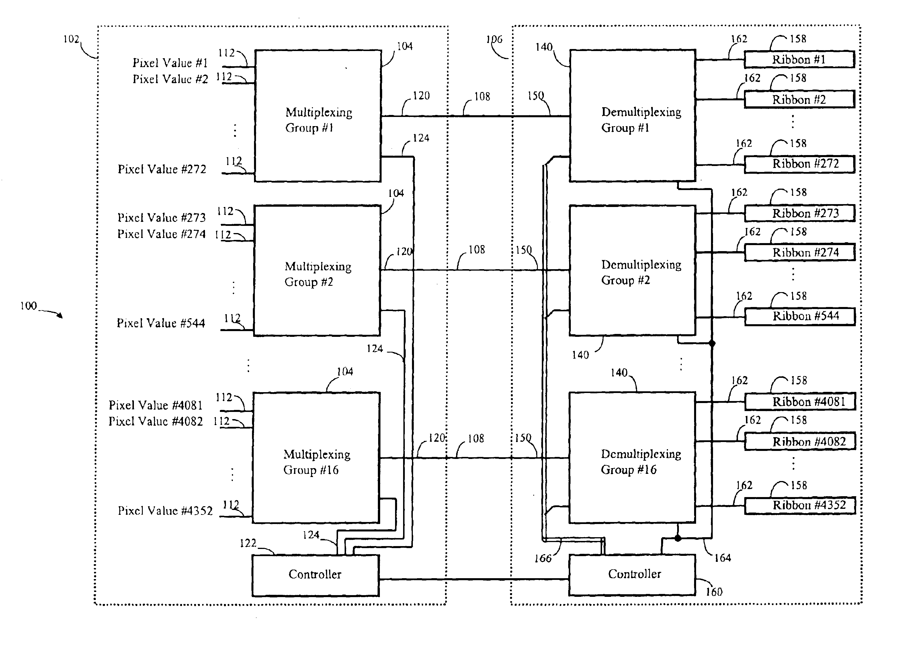
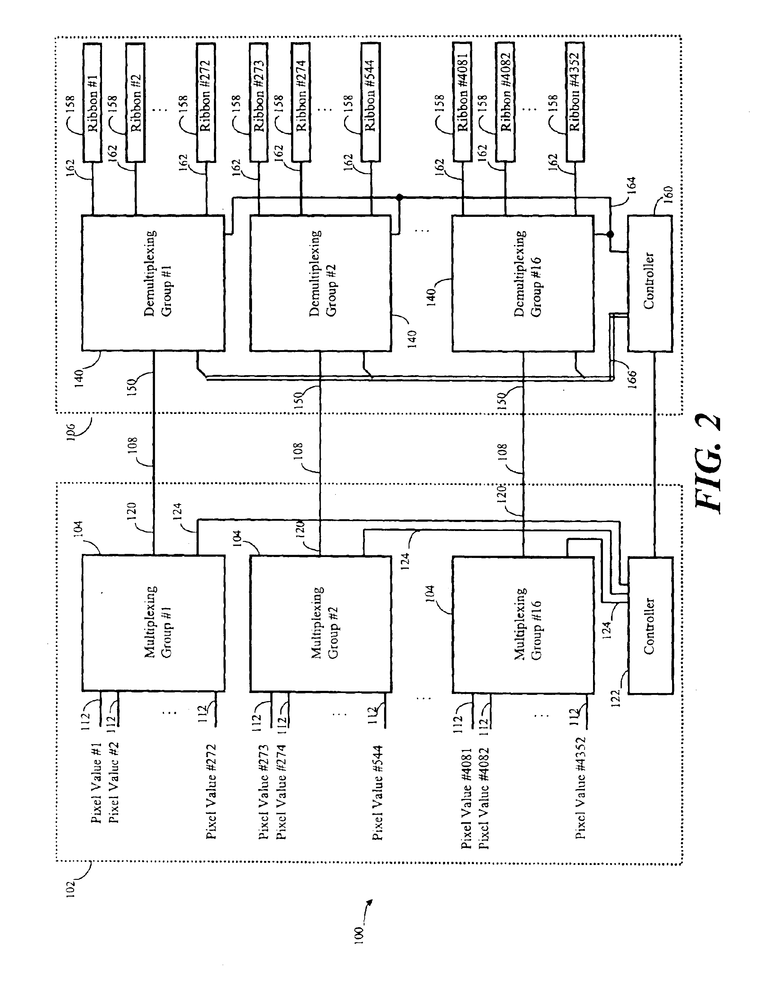
Reference will now be made to the exemplary embodiments illustrated in the drawings, and specific language will be used herein to describe the same. It will nevertheless be understood that no limitation of the scope of the invention is thereby intended. Alterations and further modifications of the inventive features illustrated herein, and additional applications of the principles of the inventions as illustrated herein, which would occur to one skilled in the relevant art and having possession of this disclosure, are to be considered within the scope of the invention.

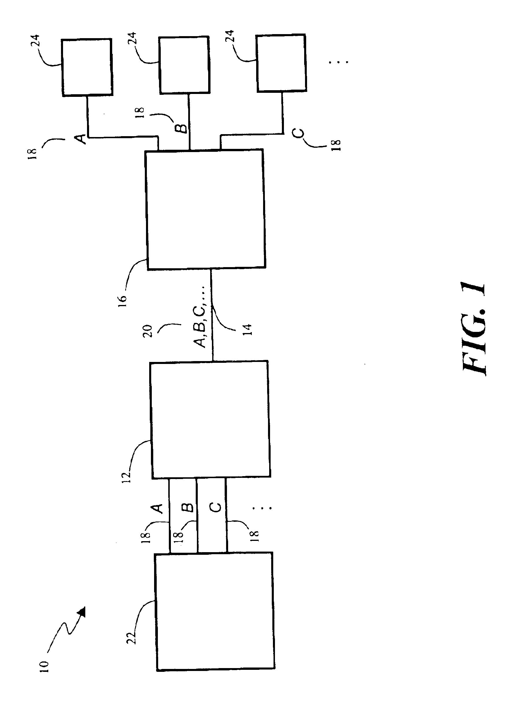
It is to be understood the term “multiplexing” used herein refers to any technique for combining two distinct electrical signals for communication through an electrical interface. It is also to be understood the term “demultiplexing” used herein refers to any corresponding technique for extracting the distinct electrical signals from a multiplexed signal. It is also to be understood the term “interconnect” refers to an...


PUM

PropertyMeasurementUnit
optical structuresaaaaaaaaaa
microscopic optical structuresaaaaaaaaaa
structuresaaaaaaaaaa

Abstract

A microscopic optical structure controller for providing singular control of individual microscopic optical structures of a microelectromechanical optical device by a multiplexed stream of individual pixel values generated by a pixel value source. The microscopic optical structure controller includes at least one interconnect coupled to the pixel value source for receiving the multiplexed stream of individual pixel values and at least one mapper communicating with the interconnect for extracting individual pixel values from the multiplexed stream and applying the individual pixel values to one or more individual microscopic optical structures according to a configurable mapping. A method and a driver for providing singular control of individual microscopic optical structures of a microelectromechanical optical device are also disclosed.

Description

BACKGROUND OF THE INVENTION1. Field of the InventionThe present invention relates generally to spatial light modulators. More particularly, the present invention relates to improved resolution in microelectromechanical optical devices.2. Related ArtSpatial light modulators (SLM) have found use in a variety of applications, including their use in image displays. Of particular interest are SLM manufactured using microelectromechanical systems technology (MEMS), such as a grating light valve (GLV) or digital mirror device (DMD). Operation of MEMS optical devices is similar, relying on mechanical deflection of microscopic optical structures fabricated on the device to reflect or diffract impinging light.For example, a grating light valve (GLV) can be used to modulate light intensity to implement a display as disclosed in U.S. Pat. No. 6,215,579 issued to Bloom et. al. The GLV is used to modulate light intensity by electrostatic deflection of long thin microscopic optical structures (“ri...

Claims


Application Information

Patent Timeline
Patent Type & Authority Patents(United States)
IPC IPC(8): G02B26/00G02B26/08G02F1/29G09G3/20G09G3/34
CPCG09G3/3433G09G3/20G09G2310/0297
Inventor WINKLER, BRET D.ELKINS, DENNIS F.TANNER, ALLEN H.
Owner EVANS & SUTHERLAND COMP
Why Eureka
Try Eureka