Multi-headed decoder structure utilizing memory array line driver with dual purpose driver device

Inactive Publication Date: 2005-02-15
SANDISK TECH LLC
View PDF21 Cites 234 Cited by
  • Summary
  • Abstract
  • Description
  • Claims
  • Application Information

AI Technical Summary

Benefits of technology

An improved decoder organization for a memory array readily interfaces to array lines, such as word lines, having extremely dense pitch, and in particular interfaces to extremely dense array lines of a three-dimensional memory array. In exemplary embodiments, a multi-headed decoder includes a group of array line driver circuits associated with a single decode node. Each array line driver circuit at times couples its associated array line, such as through a first device, to a

Problems solved by technology

In addition, since each head is controlled by its own bias generator circuits, four different circuits are required to generate the four different selected bias nodes A, B, C, and D, and four different circuits are also required to generate the four different unselected bias nodes W, X, Y, and Z. Accomplishing a group of four decoders 192 on such a small effective pitch is extremely difficult, and results in a very wide layout, if achievable at all.
Moreover, routing the four decode nodes out to the four quads 200 results in significant wiring congestion.
This approach reduces the number of “external” control circuits (i.e., outside the pitched requirement of the word lines) but at the expense of a large number of decoder circuits that must interface with the pitched word lines of the array.
Such a shared word line arrangement may result in power dissipation, particularly during a write or programming operation, which is unacceptably high.
For example, wit

Method used


Image

  • Multi-headed decoder structure utilizing memory array line driver with dual purpose driver device
  • Multi-headed decoder structure utilizing memory array line driver with dual purpose driver device
  • Multi-headed decoder structure utilizing memory array line driver with dual purpose driver device

Examples


Embodiment Construction

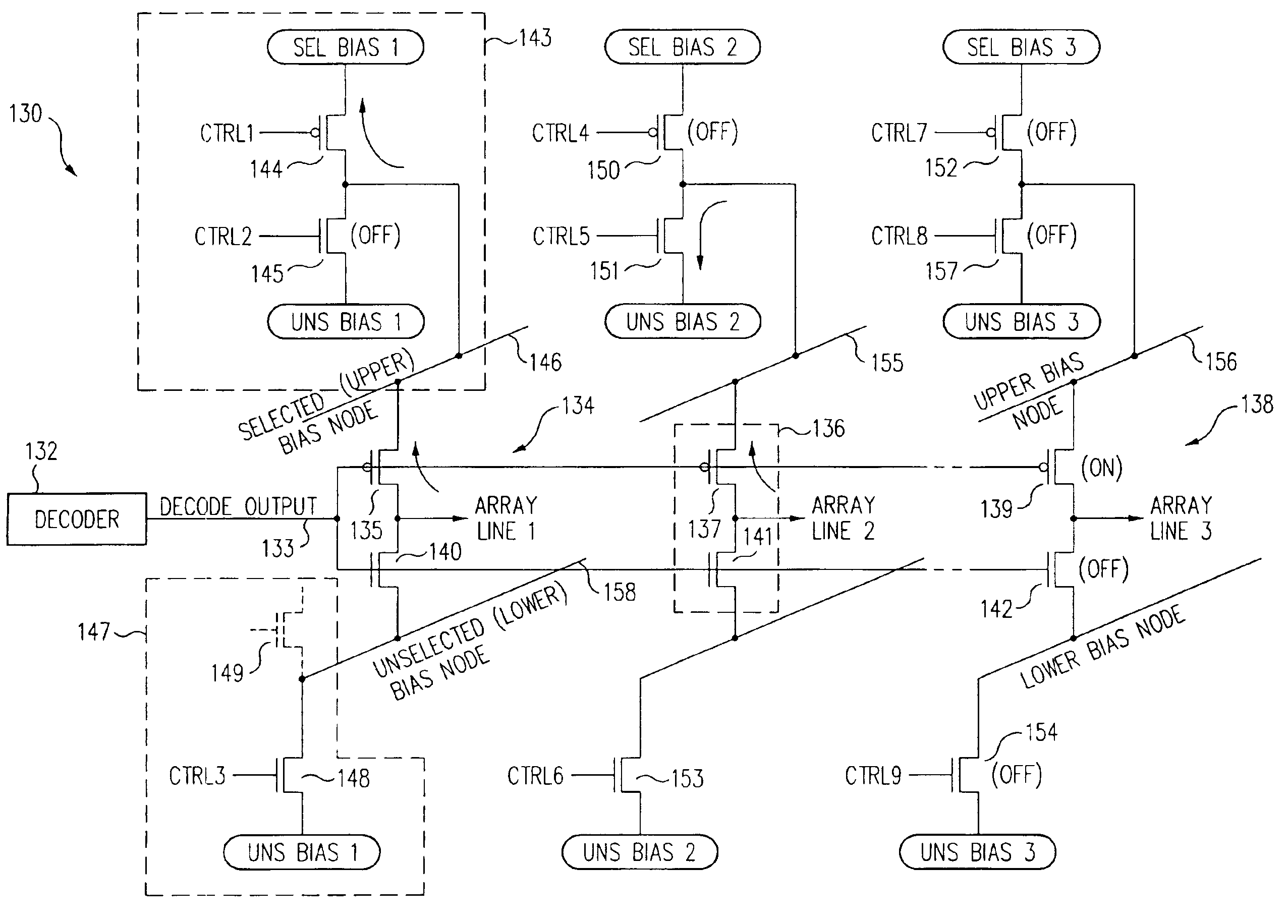
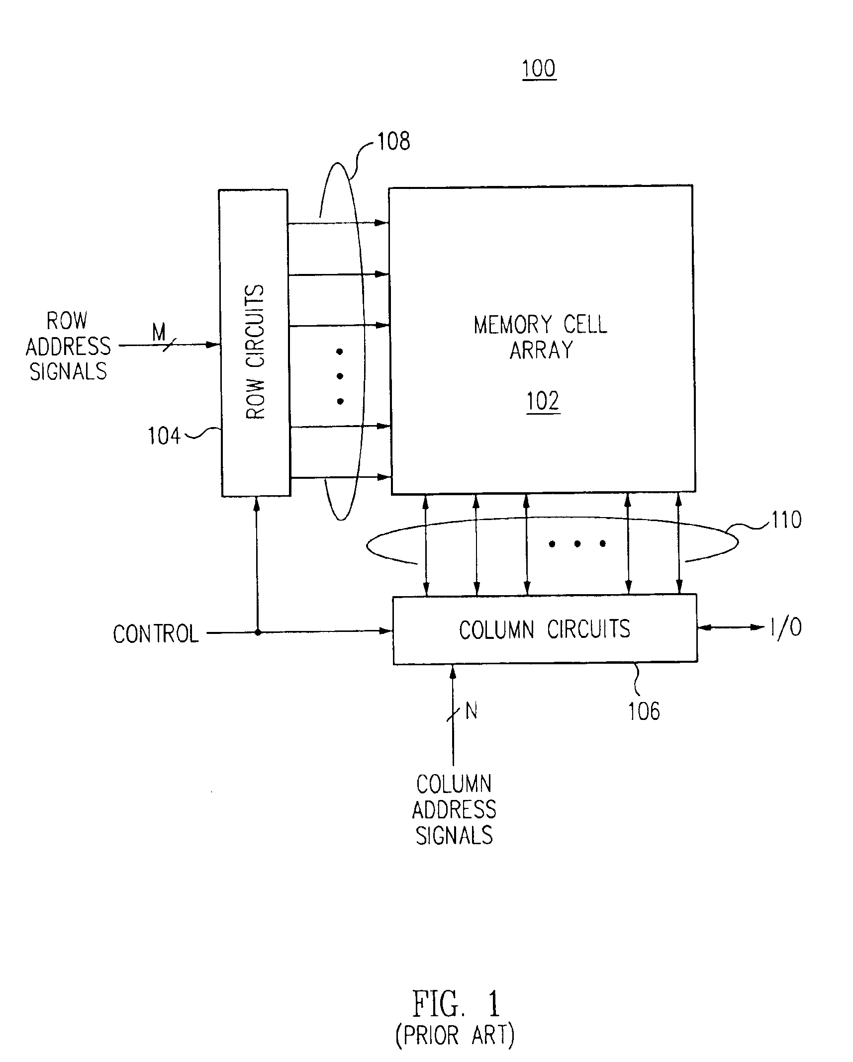
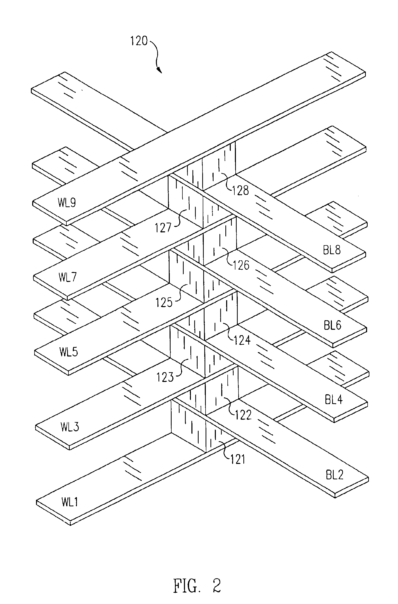
Referring now to FIG. 1, a block diagram is shown of an integrated circuit 100 including a memory array 102. In one embodiment of the invention, the memory array 102 is preferably a three-dimensional, non-volatile, field-programmable write-once memory array of passive element memory cells, although other memory arrays are also suitable and specifically contemplated, including re-writable arrays and two-dimensional arrays. As used herein, an integrated circuit having a three-dimensional memory array is assumed to be a monolithic integrated circuit, rather than an assembly of more than one monolithic integrated circuit. Each passive element memory cell within the memory array 102 is preferably a two-terminal memory cell having a steering element in series with a state change element, together connected between usually orthogonal (but not necessarily so) array terminal lines. These two elements within a memory cell may both be present before programming. Alternatively, the steering ele...


PUM


Abstract

A memory array decoder organization readily interfaces to array lines having extremely dense pitch, and in particular interfaces to extremely dense array lines of a three-dimensional memory array. In an exemplary embodiment, a multi-headed decoder includes a group of array line driver circuits associated with a single decode node. Each array line driver circuit couples its associated array line through a first device to an associated upper bias node which is generated to convey either a selected bias condition or an unselected bias condition thereon appropriate for the array line. Each array line driver circuit also couples its associated array line through a second device to an associated lower bias node which is generated to convey an unselected bias condition appropriate for the array line. The array line driver circuits for several different decode nodes may be physically arranged in one or more banks.

Description

BACKGROUNDThe present invention relates to semiconductor integrated circuits containing memory arrays, and particularly those arrays incorporating array lines having extremely small pitch, and more particularly those having a three-dimensional memory array.Semiconductor integrated circuits have progressively reduced their feature linewidths into the deep sub-micron regime. Moreover, recent developments in certain memory cell technologies have resulted in word lines and bit line having an extremely small pitch. For example, certain passive element memory cell arrays may be fabricated having word lines approaching the minimum feature size (F) and minimum feature spacing for the particular word line interconnect layer, and also having bit lines approaching the minimum feature width and minimum feature spacing for the particular bit line interconnect layer. Moreover, three-dimensional memory arrays having more than one plane of memory cells have been fabricated implanting such so-called...

Claims


Application Information

Patent Timeline
IPC IPC(8): G11C8/10G11C5/02G11C8/00H01L27/102H01L27/06
CPCG11C5/025H01L27/1021H01L27/0688G11C8/10
Inventor SCHEUERLEIN, ROY E.CROWLEY, MATTHEW P.
Owner SANDISK TECH LLC
Why Eureka
Try Eureka