Eureka AIR delivers breakthrough ideas for toughest innovation challenges, trusted by R&D personnel around the world.

Semiconductor package with lid heat spreader

Inactive Publication Date: 2005-02-22
SANOFI AVENTIS SA
View PDF11 Cites 20 Cited by
  • Summary
  • Abstract
  • Description
  • Claims
  • Application Information

AI Technical Summary

Benefits of technology

The present invention provides a semiconductor package comprising a substrate having a top surface and at least one semiconductor device attached to the top surface of the substrate. A cover is secured to the substrate creating a space between the cover and the substrate, with the semiconductor device residing within the space. The cover includes an inner chamber that is defined by a first wall and a second wall of the cover. The inner chamber contains a two-phase va

Problems solved by technology

The performance of electronic circuits and their semiconductor devices (“chips”) is limited by temperature.
Semiconductor device performance degrades when the internal temperature reaches or exceeds a particular limit.
Demands by OEMs for smaller package sizes and increased device densities has resulted in higher power densities, with the concomitant need for efficient heat dissipation becoming extremely important.
These systems often have the highest heat removal rate for a limited area, but require a considerable amount of power to operate, i.e. to be pumped to and from the heat transfer site.
Heat from the semiconductor device inside the housing boils the working fluid.
These and other prior art devices use heat pipes to transfer thermal energy away from the semiconductor device and its package, but do not provide an efficient heat spreading mechanism for distributing the thermal energy generated by hot spots on the chip across the package itself.

Method used


Image

  • Semiconductor package with lid heat spreader
  • Semiconductor package with lid heat spreader
  • Semiconductor package with lid heat spreader

Examples


Embodiment Construction

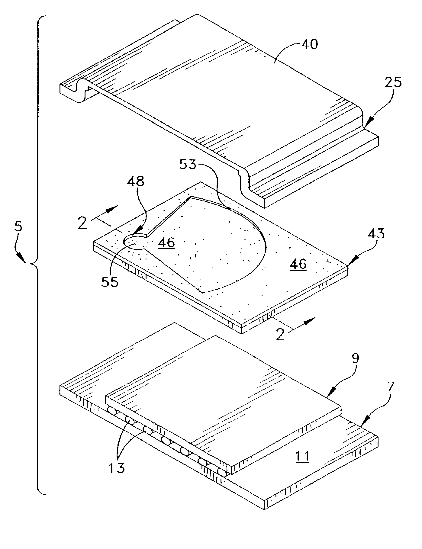
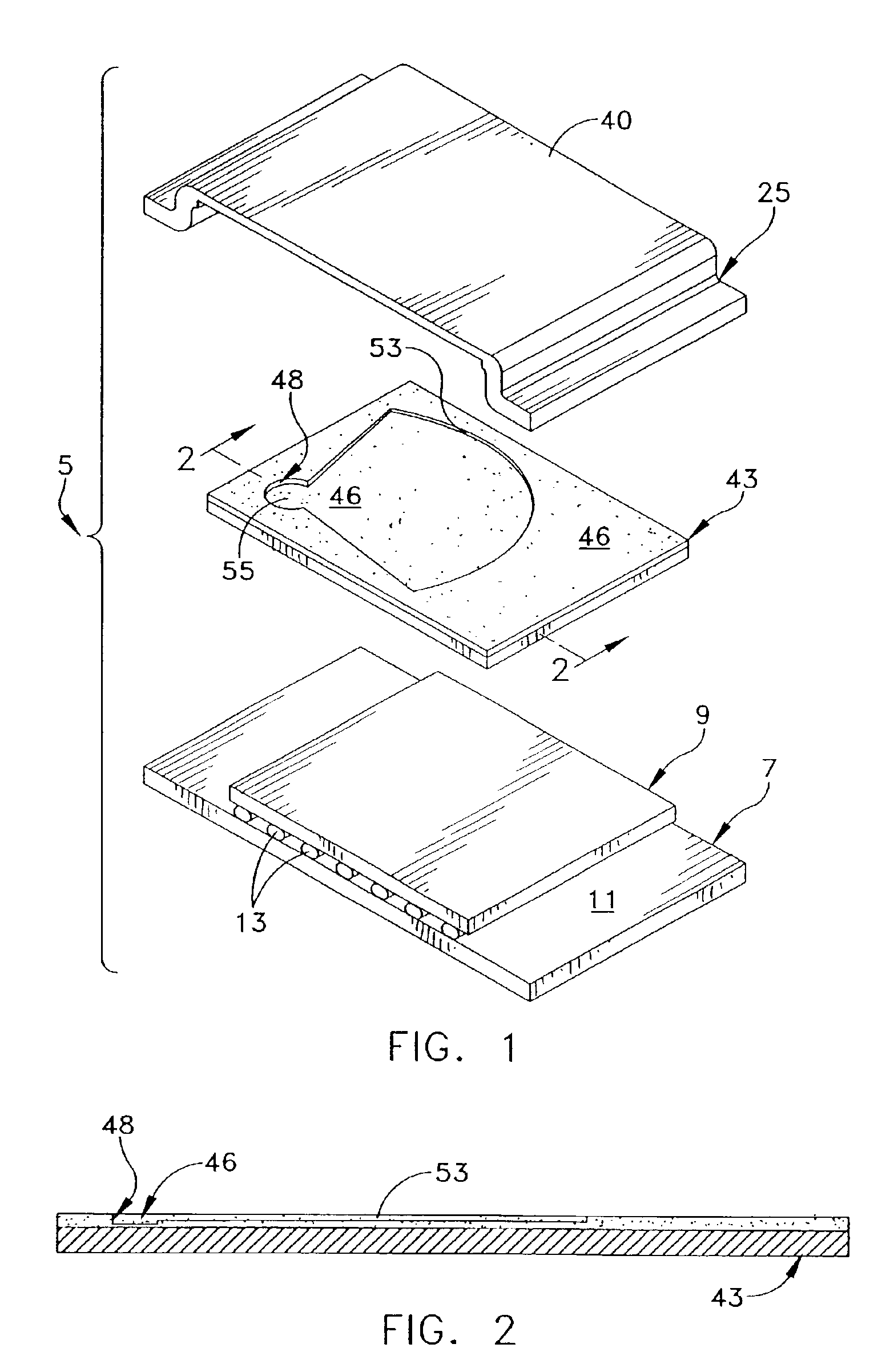
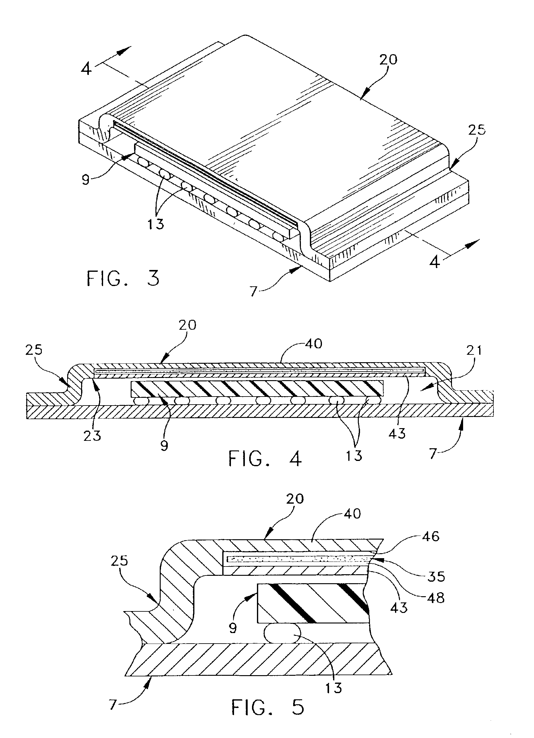
This description of preferred embodiments is intended to be read in connection with the accompanying drawings, which are to be considered part of the entire written description of this invention. In the description, relative terms such as “horizontal,”“vertical,”“up,”“down,”“top” and “bottom” as well as derivatives thereof (e.g., “horizontally,”“downwardly,”“upwardly,” etc.) should be construed to refer to the orientation as then described or as shown in the drawing figure under discussion. These relative terms are for convenience of description and normally are not intended to require a particular orientation. Terms including “inwardly” versus “outwardly,”“longitudinal” versus “lateral” and the like are to be interpreted relative to one another or relative to an axis of elongation, or an axis or center of rotation, as appropriate. Terms concerning attachments, coupling and the like, such as “connected” and “interconnected,” refer to a relationship wherein structures are secured or ...


PUM


Abstract

The invention provides a semiconductor package having a substrate, a top surface and at least one semiconductor device attached to the top surface of the substrate. A cover is secured to the substrate creating a space between the cover and the substrate, with the semiconductor device residing within the space. The cover includes an inner chamber that is defined by an upper wall and a lower wall of the cover. The cavity contains a two-phase vaporizable liquid and a wick. Advantageously, the wick on the lower wall includes at least one recess that forms a thinned wall adjacent to a high heat generation portion of the semiconductor device. In one embodiment, the wick on the lower wall includes at least one channel that communicates with at least one of the recesses.

Description

FIELD OF THE INVENTIONThe present invention generally relates to thermal management in semiconductor devices, and more particularly to a package architecture that is adapted for use with semiconductor devices to spread heat generated at hot spots.BACKGROUND OF THE INVENTIONThe performance of electronic circuits and their semiconductor devices (“chips”) is limited by temperature. Semiconductor device performance degrades when the internal temperature reaches or exceeds a particular limit. For example, in silicon integrated circuit devices, for each ten degree centigrade rise in junction temperature, the operating lifetime of the semiconductor device is decreased by a factor of at least two. Demands by OEMs for smaller package sizes and increased device densities has resulted in higher power densities, with the concomitant need for efficient heat dissipation becoming extremely important.This industry need is compounded, in next generation, highly integrated semiconductor devices by th...

Claims


Application Information

Patent Timeline
IPC IPC(8): H01L23/427H01L23/34
CPCH01L23/427H01L2224/16H01L2224/73253H01L2924/01057H01L2924/16152H01L2224/16225H01L2924/01322H01L2924/00014H01L2224/0401
Inventor ZUO, JONERNST, DONALD M.
Owner SANOFI AVENTIS SA
Why Eureka
Eureka Blog
Learn More