Design-for-test modes for a phase locked loop

Inactive Publication Date: 2005-02-22
INTELLECTUAL VENTURES HOLDING 81 LLC
View PDF3 Cites 56 Cited by
  • Summary
  • Abstract
  • Description
  • Claims
  • Application Information

AI Technical Summary

Benefits of technology

According to the invention there is provided a modified phase locked-loop (PLL) integrated with testing apparatus. The PLL in combination wit the integrated testing apparatus is

Problems solved by technology

Generally, the testing of integrated circuits presents a number of technical challenges that significantly add to the cost of development and production.
Specifically, there are two major difficulties that arise in the testing of integrated circuits.
Test structures take up additional space (i.e. chip area) that reduces the usable area of a chip or add to the overall chip area required for the end product.
Test structures also cause undesirable parasitic loading of the integrated circuit components leading to performance degradation and spurious power consumption.
Furthermore, the interface used to access the test structures is typically different from the actual integrated product interface; thus, once an integrated product is in the field it becomes difficult to identify and resolve even minor problems.
Lastly, in many cases the interface to the test struct

Method used


Image

  • Design-for-test modes for a phase locked loop
  • Design-for-test modes for a phase locked loop
  • Design-for-test modes for a phase locked loop

Examples


Embodiment Construction

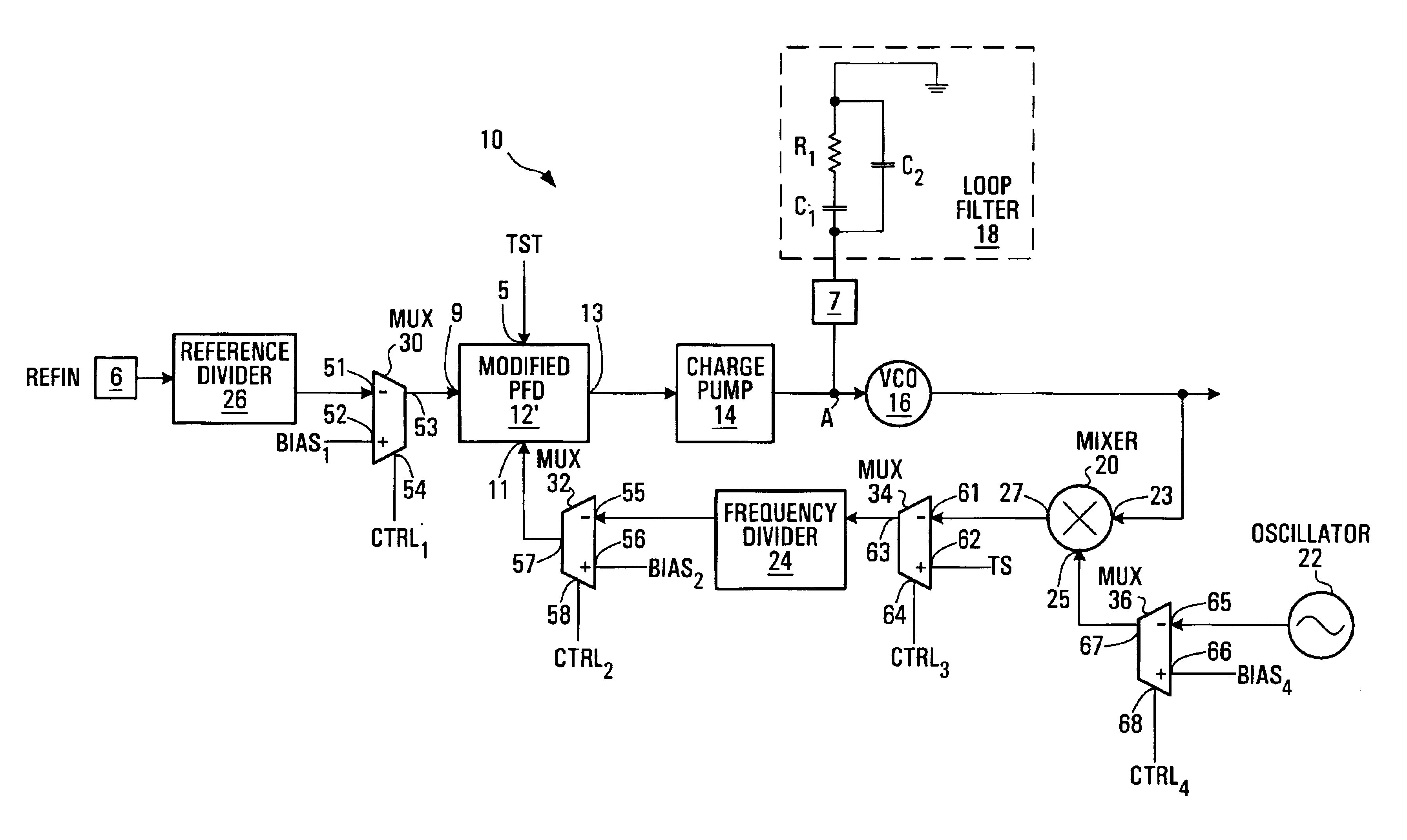
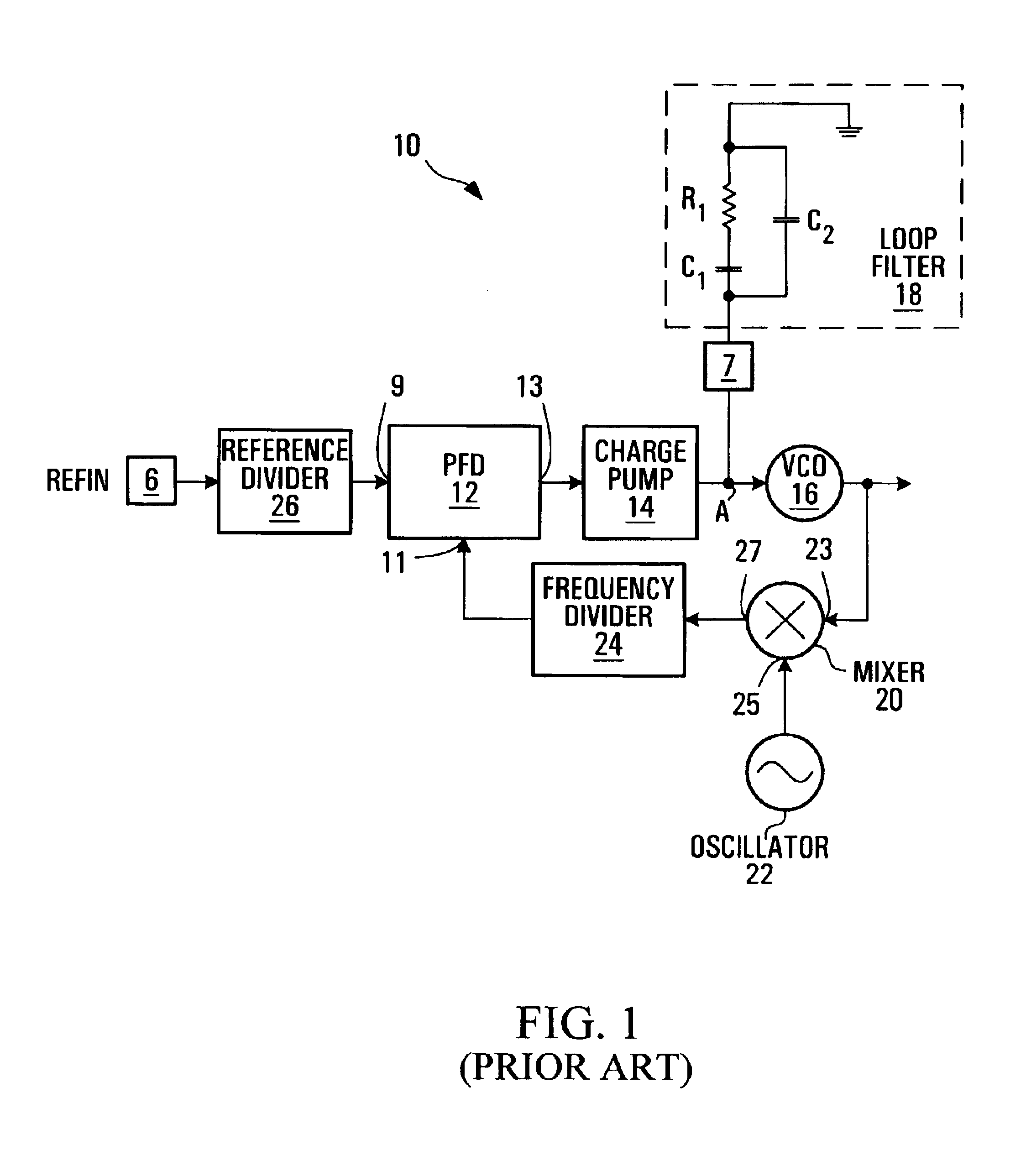
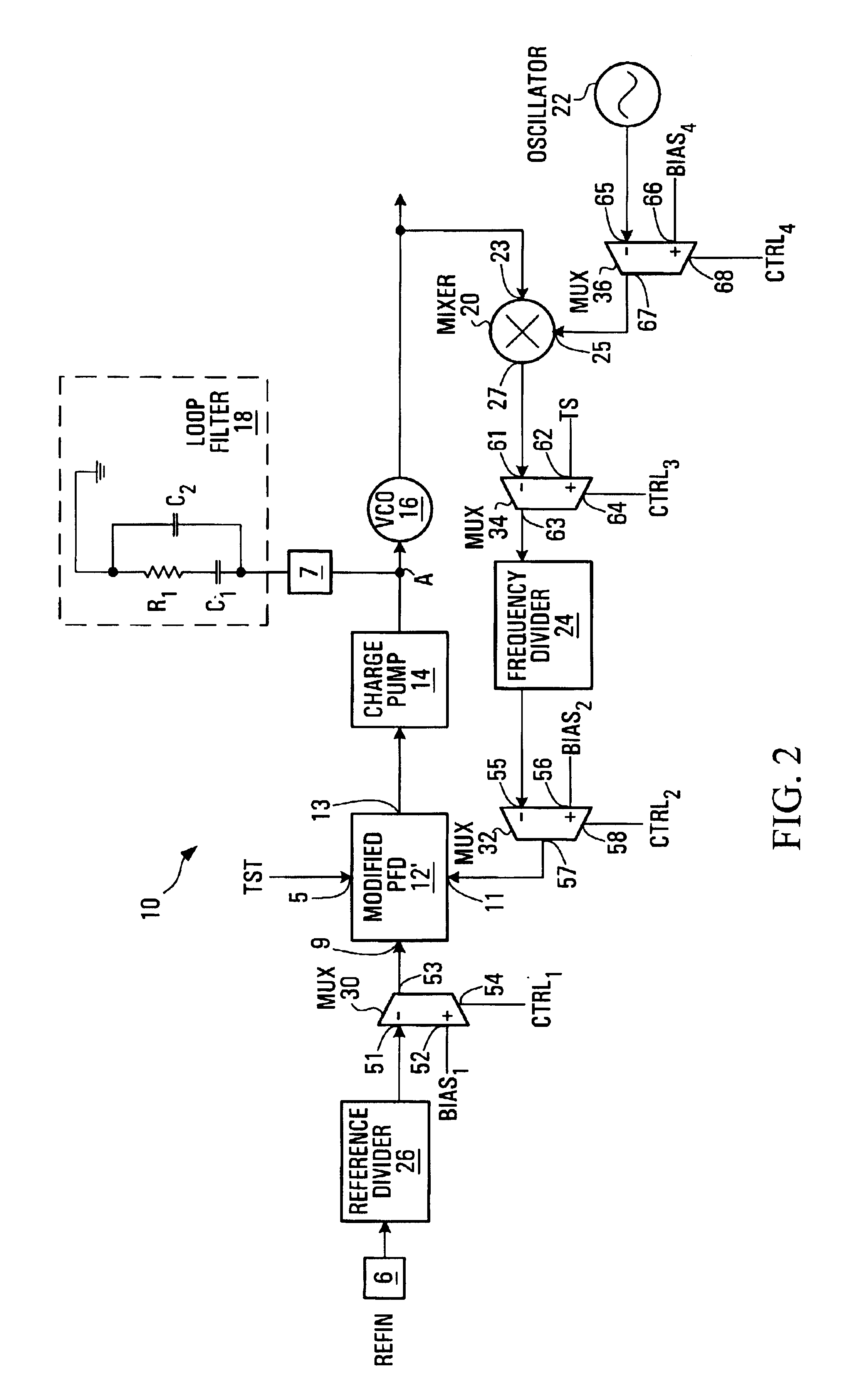
In order to produce a phase locked-loop (PLL) having integrated testing apparatus, without having the PLL suffer severe performance degradations during nominal operation nor having the combination of the PLL and testing apparatus be unnecessarily large, a modified PLL integrated with testing apparatus is provided. To that end, FIG. 2 illustrates a first embodiment of a PLL 10′ integrated onto a chip adapted according to the invention from a typical PLL 10 (also integrated on a chip) shown in FIG. 1.

The PLL 10 of FIG. 1 has a first number of circuits connected to form a loop. The circuits forming the loop (listed in order) are a phase-frequency detector (PFD) 12, a charge pump 14, a loop filter 18, a voltage-controlled oscillator (VCO) 16, a mixer 20, and a frequency divider 24, the frequency divider 24 connected to the PFD 12 to close the loop. The PLL 10 also has a reference divider 26 coupled to the PFD 12 and an oscillator 22 coupled to the mixer 20. The reference divider 26 and ...


PUM


Abstract

There is a desire to provide a testing method and apparatus that can be successfully integrated into a PLL and PLL-like circuits (e.g. frequency synthesizers, delay lock loops, etc.). It is desirable that the PLL or PLL-like circuit integrated with testing apparatus does not suffer from performance degradations during nominal (mission mode) operation. Furthermore, it is desirable that the PLL and the testing apparatus share the same interface. In order to produce a PLL having integrated testing apparatus, without having the PLL suffer severe performance degradations during nominal operation nor having the combination of the PLL and testing apparatus be unnecessarily large, a modified PLL integrated with testing apparatus is provided.

Description

FIELD OF THE INVENTIONThe present invention relates to the testing of integrated circuits and in particular to the testing of fully integrated phase locked loops.BACKGROUNDGenerally, the testing of integrated circuits presents a number of technical challenges that significantly add to the cost of development and production. Specifically, there are two major difficulties that arise in the testing of integrated circuits. The first is accessibility to the individual components integrated onto the chip. The second is to provide complete test coverage while minimizing the added test structures on the chip required for testing all of the integrated product components.Test structures take up additional space (i.e. chip area) that reduces the usable area of a chip or add to the overall chip area required for the end product. Test structures also cause undesirable parasitic loading of the integrated circuit components leading to performance degradation and spurious power consumption. Further...

Claims


Application Information

Patent Timeline
IPC IPC(8): G01R31/28G01R31/317
CPCG01R31/2824G01R31/31725G01R31/31716G01R31/2884
Inventor TONER, MICHAEL F.
Owner INTELLECTUAL VENTURES HOLDING 81 LLC
Why Eureka
Try Eureka