Method and system for forming a semiconductor device

a semiconductor and device technology, applied in the field of semiconductor devices, can solve the problems of added complexity, inapplicability, and difficulty in the accuracy of optical alignment,

Inactive Publication Date: 2005-03-01
APPLIED MATERIALS INC
View PDF6 Cites 43 Cited by
  • Summary
  • Abstract
  • Description
  • Claims
  • Application Information

AI Technical Summary

Benefits of technology

The invention includes a method and system for forming a semiconductor device. The invention involves the utilization of a stamping tool to generate three-dimensional resist structures whereby thin film patterning steps can be transferred to the resist in a single molding step and subse

Problems solved by technology

Although, it is possible to use optical alignments in a roll-to-roll process it is not practical for several reasons.
First, it adds additional complexity since the fundamental imprint lithography process is not optical.
Next, the lack of planarity of the substrate in a roll-to-roll environment causes difficulties in the accuracy with which optical alignments can

Method used


Image

  • Method and system for forming a semiconductor device
  • Method and system for forming a semiconductor device
  • Method and system for forming a semiconductor device

Examples


Embodiment Construction

The present invention relates to a method and system for forming a semiconductor device. The following description is presented to enable one of ordinary skill in the art to make and use the invention and is provided in the context of a patent application and its requirements. Various modifications to the preferred embodiment and the generic principles and features described herein will be readily apparent to those skilled in the art. Thus, the present invention is not intended to be limited to the embodiment shown but is to be accorded the widest scope consistent with the principles and features described herein.

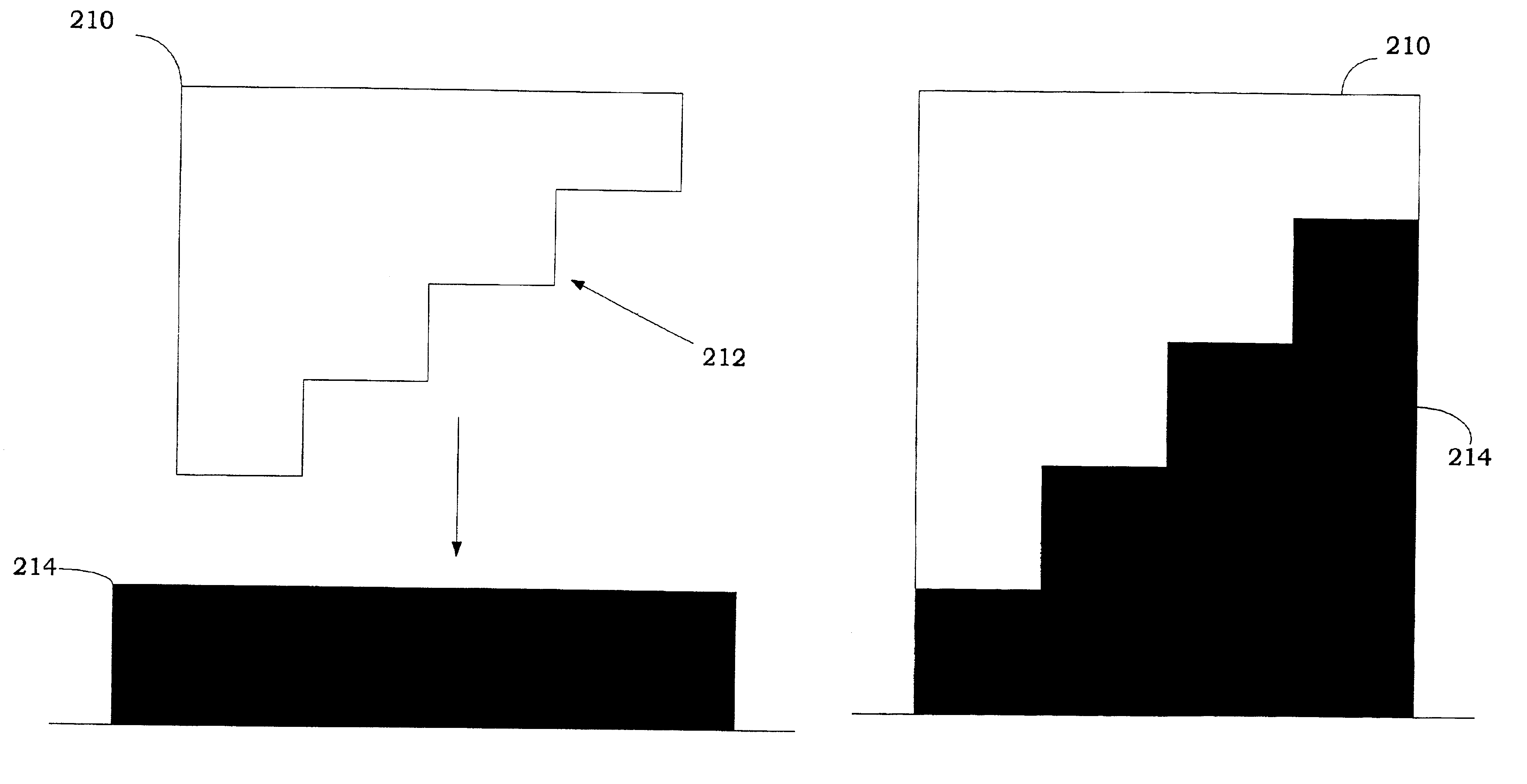
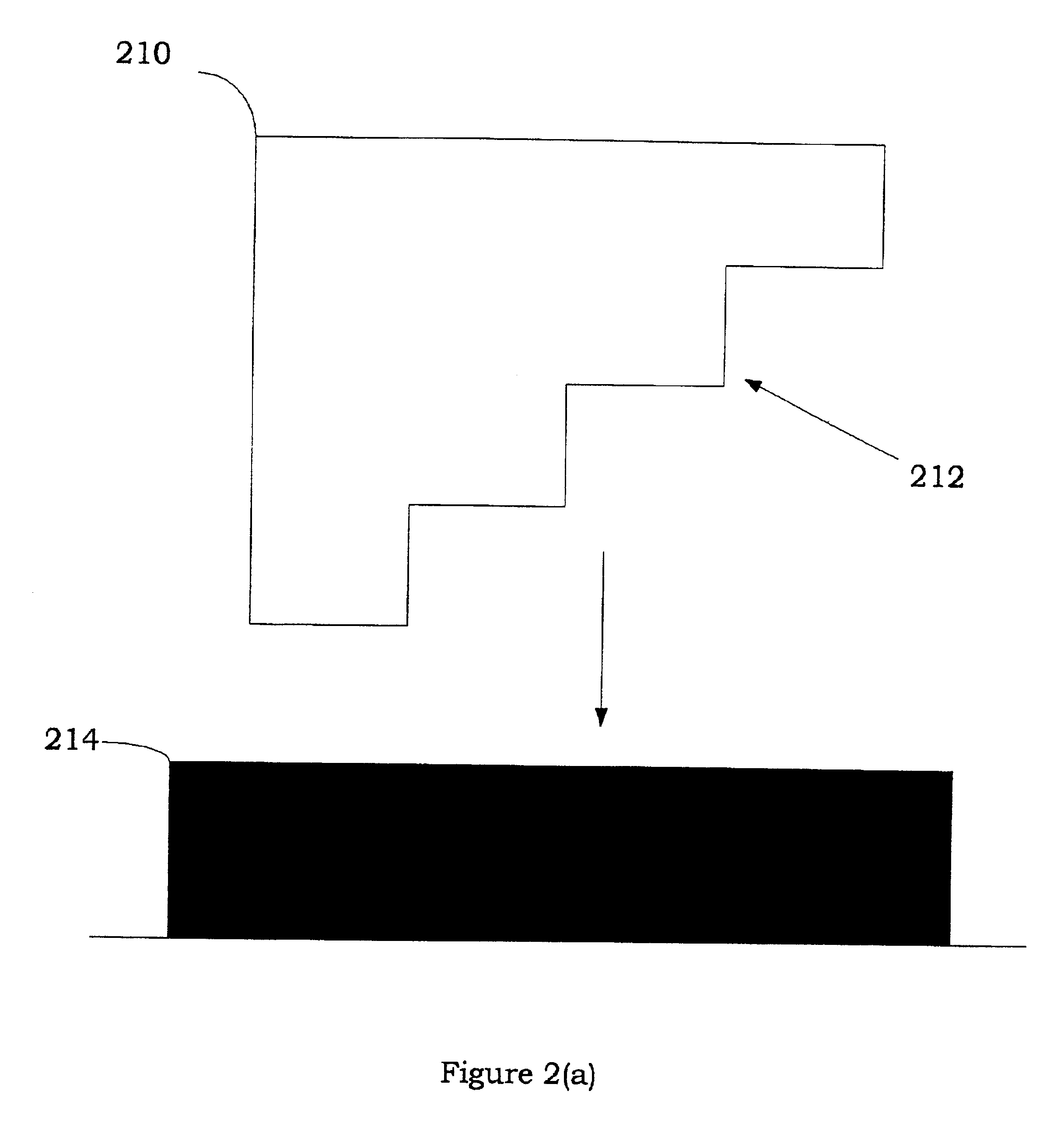
As shown in the drawings for purposes of illustration, the invention is a method and system for forming a semiconductor device. The invention involves the utilization of a stamping tool to generate three-dimensional resist structures whereby a plurality of patterns can be transferred to the resist in a single molding step and subsequently revealed in later processing steps....


PUM

PropertyMeasurementUnit
Flexibilityaaaaaaaaaa
Electrical conductoraaaaaaaaaa
Heightaaaaaaaaaa

Abstract

A method and system for forming a semiconductor device is provided. The method and system involves the utilization of a stamping tool to generate three-dimensional resist structures whereby thin film patterning steps can be transferred to the resist in a single molding step and subsequently revealed in later processing steps. Accordingly, the alignments between successive patterning steps can be determined by the accuracy with which the stamping tool has been fabricated, regardless of the dilations or contractions that can take place during the fabrication process.

Description

FIELD OF INVENTIONThe present invention relates generally to the field of semiconductor devices and more particularly to a method and system for forming a semiconductor device.BACKGROUND OF THE INVENTIONThere is currently a strong trend toward downsizing existing structures and fabricating smaller structures. This process is commonly referred to as microfabrication. One area in which microfabrication has had a sizeable impact is in the microelectronic area. In particular, the downsizing of microelectronic structures has generally allowed the structures to be less expensive, have higher performance, exhibit reduced power consumption, and contain more components for a given dimension. Although microfabrication has been widely active in the electronics industry, it has also been applied to other applications such as biotechnology, optics, mechanical systems, sensing devices, and reactors.One method employed in the microfabrication process is imprint lithography. Imprint lithography is ...

Claims


Application Information

Patent Timeline
IPC IPC(8): B41C3/00B81C1/00B81C5/00G03F7/00H01L21/00H01L21/02H01L21/027H01L21/302H01L51/40H01L21/311H01L51/05B81C99/00H01L21/033H01L21/308
CPCB82Y10/00B82Y40/00G03F7/0002H01L21/3085H01L21/0334H01L21/0335H01L21/0273
Inventor TAUSSIG, CARL PHILLIPMEI, PING
Owner APPLIED MATERIALS INC
Why Eureka
Try Eureka