
Measurement of wafer temperature in semiconductor processing chambers

a technology of semiconductor and temperature measurement, which is applied in the direction of heat measurement, semiconductor/solid-state device testing/measurement, instruments, etc., can solve the problems of inability to quickly and reliably measure the temperature of semiconductor wafers in lamp-heated degas chambers, cumbersome, and inability to measure in-situ temperatur

Active Publication Date: 2005-03-08
TEXAS INSTR INC
View PDF5 Cites 32 Cited by
  • Summary
  • Abstract
  • Description
  • Claims
  • Application Information

AI Technical Summary

Benefits of technology

An apparatus and method for measuring the temperature of a semiconductor wafer is provided. A first coil is placed in a semiconductor processing tool and connected to an electronic apparatus. A semiconductor wafer is mounted in the semiconductor tool and held in place by mounts in close proximity to the first coil. Alternating current is supplied to the first coil through the electronic

Problems solved by technology

Rapid and reliable wafer temperature measurement is currently not available in lamp-heated degas chambers.
In addition, the built-in thermocouple is often affected by emissivity variation in the system.
Dummy wafers with thermocouples built-in to the wafer are used but are very cumbersome and not suitable for in-situ temperature measurements during single wafer processing.
Temperatures measurements made using wafers carrying CMOS-based temperature-sensor arrays are limited to temperatures less than 150° C. by the battery, the battery life, and the circuitry required for such measurements.
Current single wafer manufacturing tools pose special problems in obtaining accurate and reproducible temperature measurements.
The pyrometers used in a vast majority of such systems are affected by emissivity variations that introduce inaccuracies in the temperature measurement.

Method used


Image

  • Measurement of wafer temperature in semiconductor processing chambers
  • Measurement of wafer temperature in semiconductor processing chambers
  • Measurement of wafer temperature in semiconductor processing chambers

Examples


Embodiment Construction

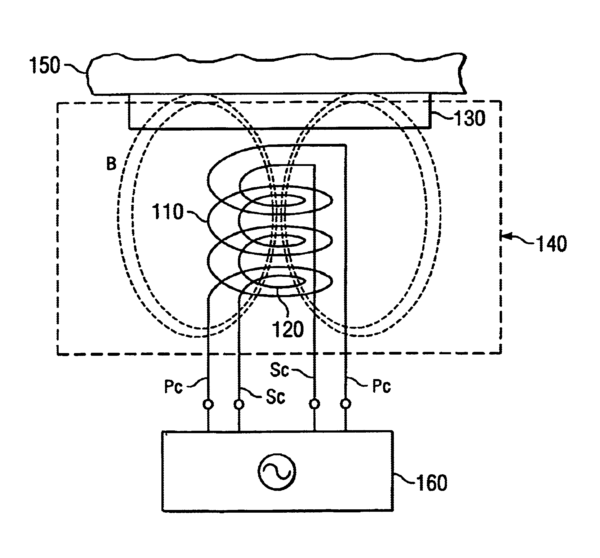
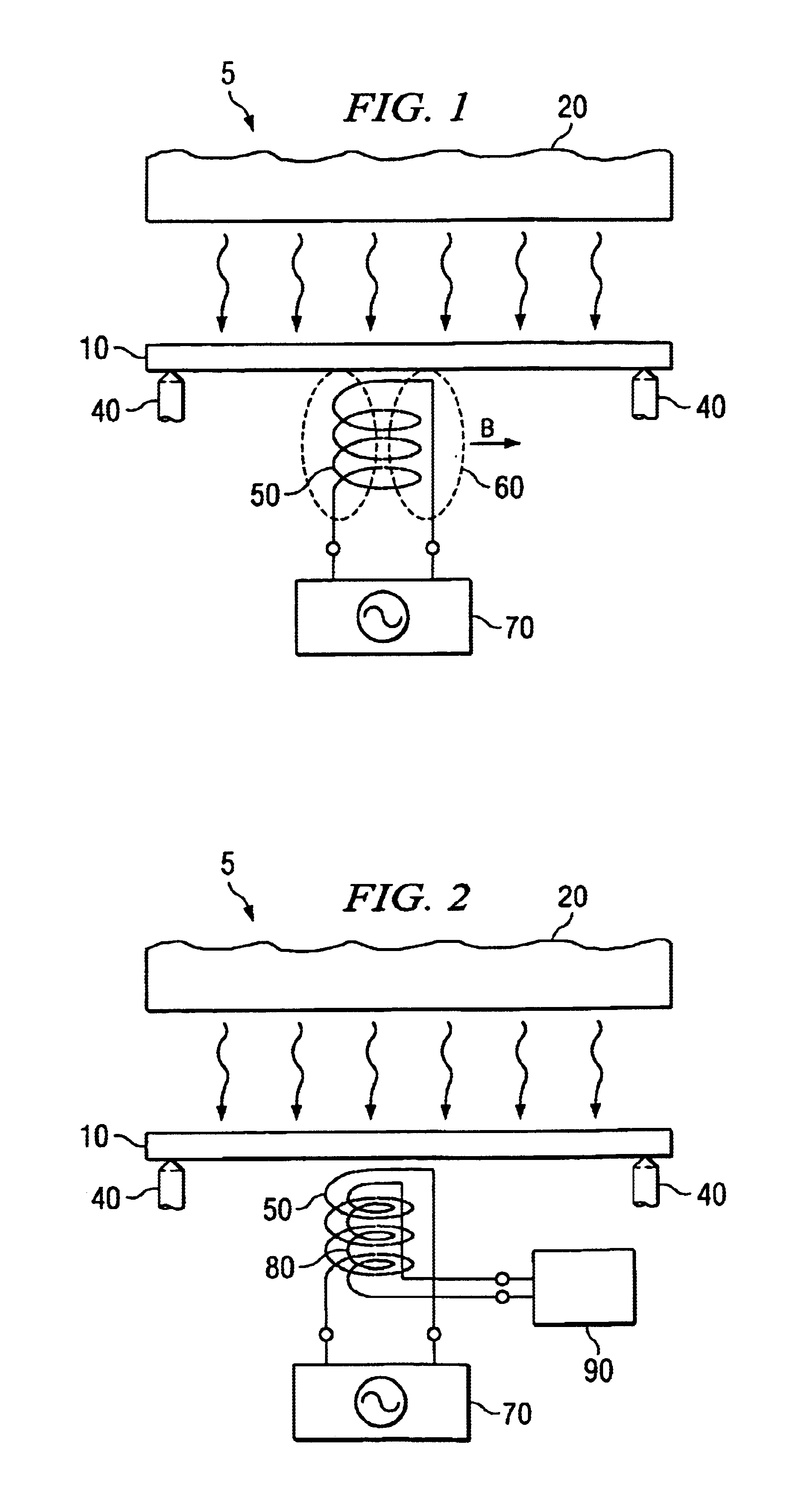
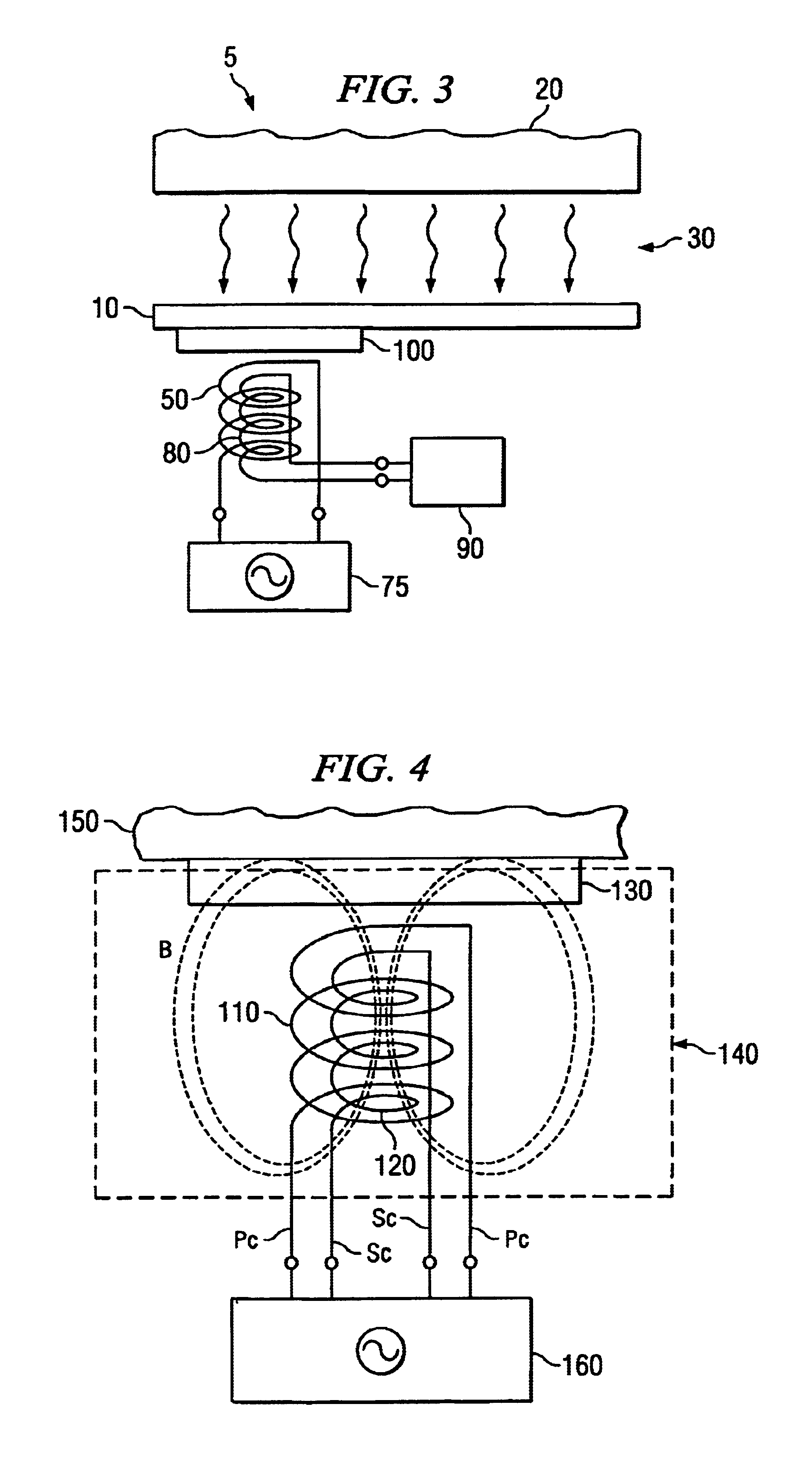
While the following description of the instant invention revolves around FIGS. 1-4, the instant invention can be utilized in any temperature measurement configuration. The methodology of the instant invention provides an improved apparatus and method for obtaining the temperature of a semiconductor wafer during processing.

Shown in FIG. 1 is a schematic diagram of a wafer temperature measuring apparatus according to an embodiment of the instant invention. A semiconductor wafer 10 is placed in a semiconductor processing tool 5. Various components of the semiconductor processing tool have been omitted from all the Figures for clarity. The semiconductor wafer 10 is held in place by wafer mounts 40 and is heated using a heat source 20. The wafer mounts 40 are depicted in FIG. 1 as pins but the instant invention is intended to encompass any method of holding the wafer 10 in place during processing. The heat source 20 represents any method for heating the wafer during processing including ...


PUM


Abstract

A coil (50) is placed adjacent to a semiconductor wafer (10). An AC excitation current is used to create a changing electromagnetic field (60) is the wafer (10). The wafer is heated by a heat source (20) and the conductivity of the wafer (10) will change as a function of the wafer temperature. Induced eddy currents will cause the inductance of the coil (50) to change and the temperature of the wafer (10) can be determined by monitoring the inductance of the coil (50).

Description

FIELD OF THE INVENTIONThe invention is generally related to the field of semiconductor processing and more specifically to method and apparatus for measuring the temperature of a semiconductor wafer during wafer processing.BACKGROUND OF THE INVENTIONThe processing of semiconductor wafers to form integrated circuits often requires a precise control of temperature. As device dimensions are reduced the control of the wafer temperature during processing is becoming a more critical component in maintaining high integrated circuit manufacturing yields. In particular with the increased use of ultra-low K (ULK) dielectrics, wafer-degas processing and temperature control are becoming more critical. Rapid and reliable wafer temperature measurement is currently not available in lamp-heated degas chambers.A number of methods are currently being used to obtain the semiconductor wafer temperature during processing. Thermocouples built-in to the tools are often used but are usually not in direct c...

Claims


Application Information

Patent Timeline
IPC IPC(8): G01K7/00G01K7/36H01L21/00
CPCG01K7/00G01K7/36H01L21/67248
Inventor PAPA RAO, SATYAVOLU S.GRUNOW, STEPHANRUSSELL, NOEL M.
Owner TEXAS INSTR INC
Features
  • Generate Ideas
  • Intellectual Property
  • Life Sciences
  • Materials
  • Tech Scout
  • Unparalleled Data Quality
  • Higher Quality Content
  • 60% Fewer Hallucinations
Learn More