Supercharge Your Innovation With Domain-Expert AI Agents!

Semiconductor device having memory cell portion and manufacturing method thereof

a technology of memory cell and semiconductor device, which is applied in the direction of semiconductor device, electrical apparatus, transistor, etc., can solve the problems of difficult to form contacts between interconnections without causing short circuits, and achieve the effect of ensuring short circuit margin, reducing punch-through margin of transistor, and enhancing current driving capability

Inactive Publication Date: 2005-03-08
RENESAS ELECTRONICS CORP
View PDF4 Cites 4 Cited by
  • Summary
  • Abstract
  • Description
  • Claims
  • Application Information

AI Technical Summary

Benefits of technology

The present invention provides a semiconductor device with a data holding portion and a peripheral circuit portion that offer enhanced short circuits margin and current driving capability. The method for manufacturing the semiconductor device includes forming gate interconnections and first impurity regions in the data holding portion and peripheral circuit portion, followed by the formation of first sidewall nitride films and first interlayer insulating film. Third impurity regions are then selectively formed in the peripheral circuit portion. The semiconductor device also includes metal silicide films on all contact plugs and the surface of the semiconductor substrate in the peripheral circuit portion where the third impurity regions are formed. These features prevent reduction of punch-through margin of transistors and improve the burying characteristics and refresh characteristics of the semiconductor device.

Problems solved by technology

Because of the increase in integration degree of semiconductor devices, and because of the miniaturization of memory cells particularly in semiconductor storage devices, it is becoming difficult to form contacts between interconnections without causing short circuits.

Method used


Image

  • Semiconductor device having memory cell portion and manufacturing method thereof
  • Semiconductor device having memory cell portion and manufacturing method thereof
  • Semiconductor device having memory cell portion and manufacturing method thereof

Examples


Embodiment Construction

GS. 36 to 41 are cross-sectional views used to describe a sequence of process steps for manufacturing a semiconductor device according to a fourth preferred embodiment of the invention;

[0027]FIGS. 42 to 45 are cross-sectional views used to describe a sequence of process steps for manufacturing a semiconductor device according to a fifth preferred embodiment of the invention; and

[0028]FIGS. 46 to 52 are cross-sectional views used to describe a sequence of process steps for manufacturing a semiconductor device according to a sixth preferred embodiment of the invention.

DESCRIPTION OF THE PREFERRED EMBODIMENTS

[0029]A. First Preferred Embodiment

[0030]A first preferred embodiment of the present invention is now described referring to FIGS. 1 to 24.

[0031]A-1. Manufacturing Method

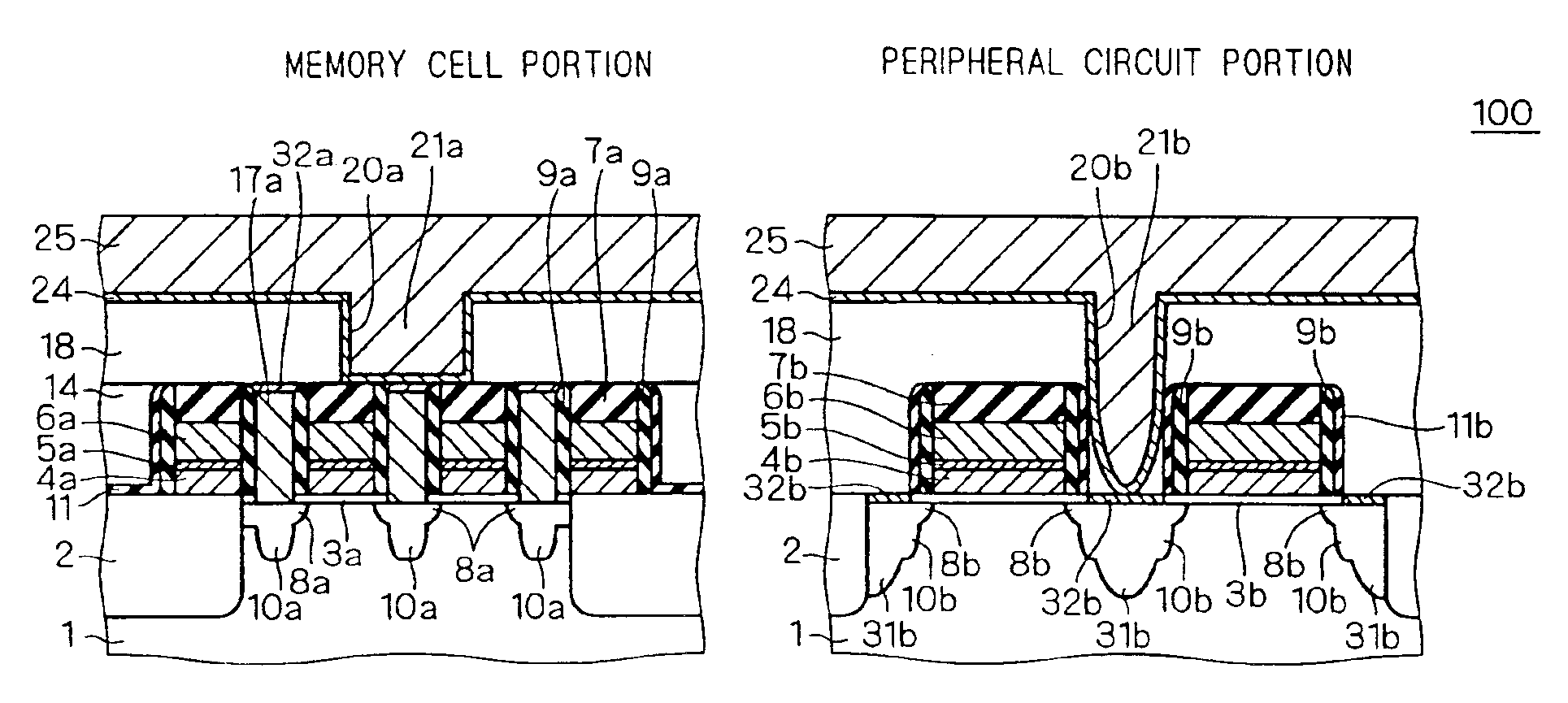
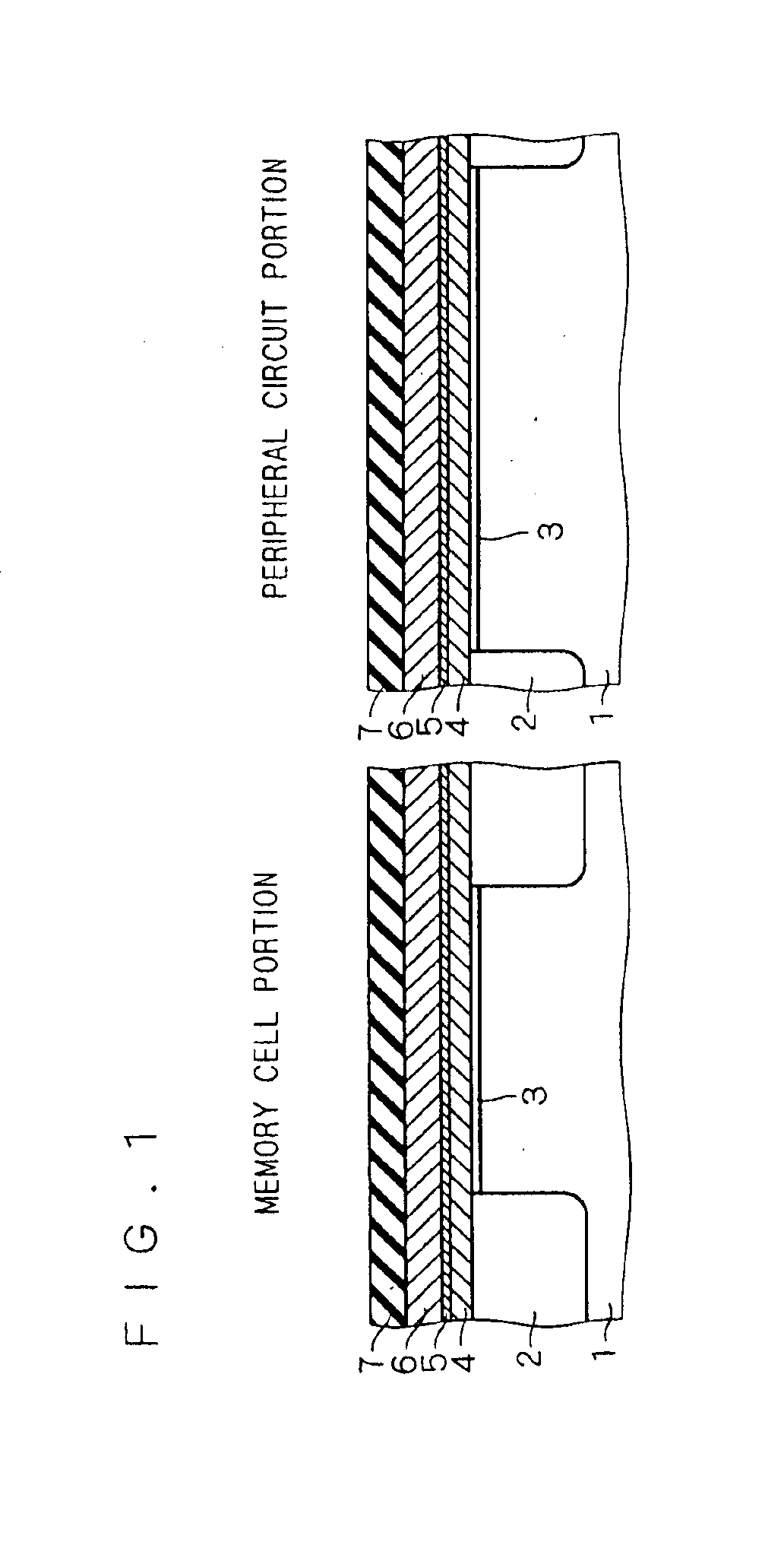
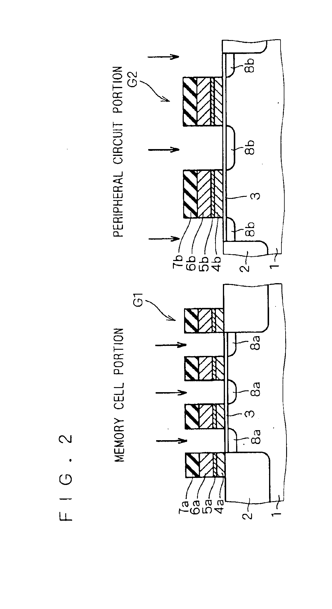
[0032]Referring to the cross-sectional views of FIGS. 1 to 16 showing a sequence of manufacturing process steps, a method for manufacturing a DRAM (Dynamic Random Access Memory) 100 is now described. The structure ...


PUM


Abstract

A semiconductor device having a memory cell portion and a peripheral circuit portion is provided which achieves suppression of reduction of punch-through margin of transistors in the peripheral circuit portion and offers ensured short margin and enhanced current driving capability. After a high-temperature (800° C. to 1000° C.) thermal treatment that is performed to improve burying characteristics after formation of an interlayer insulating film, and also after a high-temperature (800° C. to 1000° C.) thermal treatment that is performed to enhance refresh characteristics after formation of contact plugs in the memory cell portion, a silicon oxide film and insulating film formed on a semiconductor substrate in the peripheral circuit portion are removed by anisotropic dry-etching, leaving the insulating film as sidewall insulating films on sides of sidewall nitride films. Then an impurity ion implantation process is performed using gate interconnections as implant masks to form source / drain regions in the peripheral circuit portion.

Description

BACKGROUND OF THE INVENTION[0002]1. Field of the Invention[0003]The present invention relates to semiconductor devices, and particularly to a semiconductor device having a memory cell portion.[0004]2. Description of the Background Art[0005]Because of the increase in integration degree of semiconductor devices, and because of the miniaturization of memory cells particularly in semiconductor storage devices, it is becoming difficult to form contacts between interconnections without causing short circuits.[0006]In order to form contacts without causing short circuits with interconnections, a method called self-alignment is often adopted. Contacts formed by the self-alignment technique are called self-aligned contacts (SAC).[0007]In memory cell portions, in order to increase short circuits margin, it is common to form contacts by SAC etching using etching masks with large opening ratios, called bar-type or line-type, instead of hole-shaped ones, which is followed by chemical mechanical ...

Claims


Application Information

Patent Timeline
Patent Type & Authority Patents(United States)
IPC IPC(8): H01L21/70H01L27/115H01L21/8239H01L21/8247H10B12/00H10B69/00H10B99/00
CPCH01L27/115H01L27/1052H01L27/11543H01L27/11526H10B41/40H10B41/48H10B69/00H10B12/00
Inventor TERAUCHI, TAKASHISHIRATAKE, SHIGERU
Owner RENESAS ELECTRONICS CORP
Features
  • R&D
  • Intellectual Property
  • Life Sciences
  • Materials
  • Tech Scout
  • Unparalleled Data Quality
  • Higher Quality Content
  • 60% Fewer Hallucinations
Learn More