Plasma display panel that is operable to suppress the reflection of extraneous light, thereby improving the display contrast

a display panel and display technology, applied in the field of plasma display panels, can solve the problems of significantly low display contrast, and achieve the effects of reducing resistance, reducing production costs, and reducing voltage drop

Inactive Publication Date: 2005-03-08
PANASONIC CORP
View PDF21 Cites 7 Cited by
  • Summary
  • Abstract
  • Description
  • Claims
  • Application Information

AI Technical Summary

Benefits of technology

This configuration makes it possible to suppress the reflection of extraneous light because the black-colored first conductive layer is formed on the transparent first insulating substrate, thereby improving the display contrast and the panel characteristics. Deterioration in the conductivity due to the black color of the first conductive layer can be compensated for by the second conductive layer which has a low resistivity.
With this configuration, a black conductive film which does not reflect light can be formed and, even when float glass of lower production cost is used for the transparent first insulating substrate, there occurs no yellowish discoloration due to reaction of light transmitted through the transparent electrode and the float glass, thus enabling almost complete blackening.
The second conductive layer contains silver. This makes it possible to form a conductive film of lower resistivity which, when a voltage is applied, causes lower voltage drop and lower time constant.
The second conductive layer has a width not greater than that of the first conductive layer. This eliminates the possibility of the second conductive layer being beyond the edge of the first conductive layer even when the first conductive layer and the second conductive layer are misaligned when formed. Consequently, reflection of light by the second conductive layer can be completely eliminated even when misalignment occurs.
The second conductive layer extends to a terminal portion of the first insulating substrate to be connected with an external electrode. Thus, because only an effective display area can be blackened and the bonding strength with the float glass which makes the transparent fast insulating substrate can be increased, connection with external circuits can be made more stable and reliable.
Also, the second conductive layer includes a plurality of layers. This configuration makes it possible to form a conductive film of lower resistivity, and to form a film which shuts off the transfer of silver below the conductive layer that contains silver.

Problems solved by technology

Consequently, extraneous light is reflected on the surface of the conductive layers 52b, 53b as indicated by a solid line in FIG. 8, resulting in a problem of significantly low contrast of the display.

Method used


Image

  • Plasma display panel that is operable to suppress the reflection of extraneous light, thereby improving the display contrast
  • Plasma display panel that is operable to suppress the reflection of extraneous light, thereby improving the display contrast
  • Plasma display panel that is operable to suppress the reflection of extraneous light, thereby improving the display contrast

Examples


embodiment 1

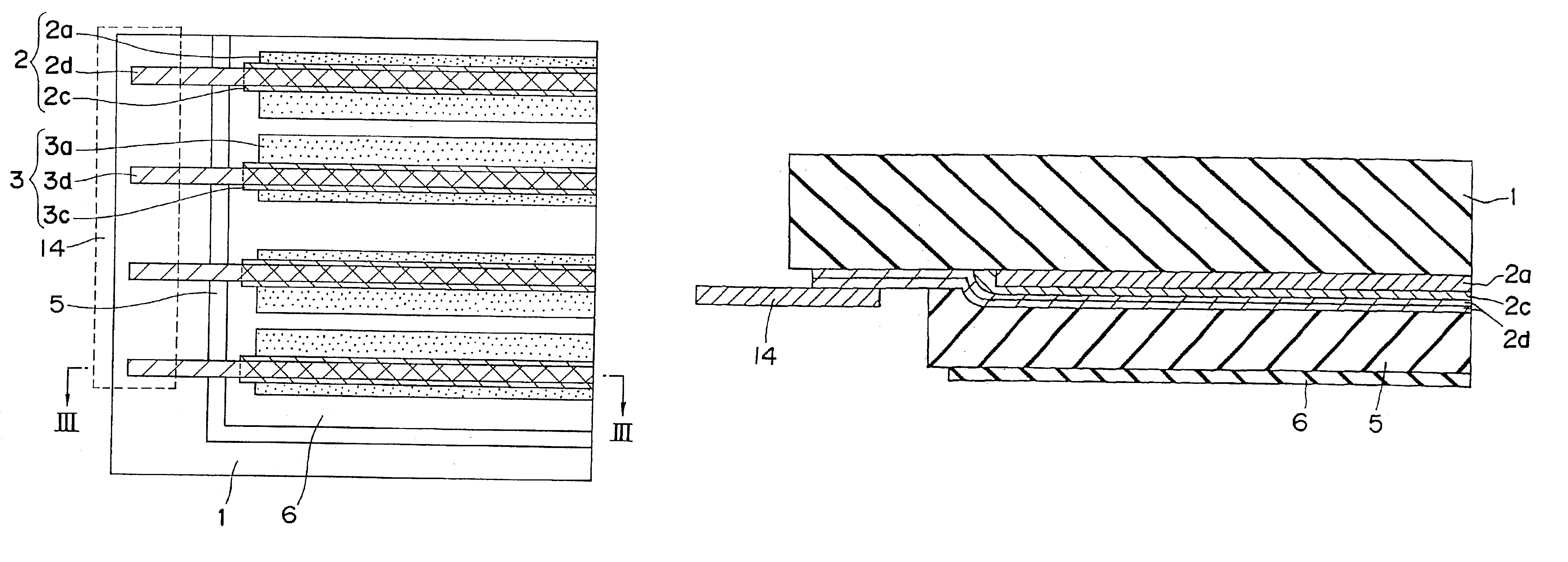
FIG. 1 is a partially cutaway perspective view of an AC type plasma display panel according to the first embodiment of the present invention.

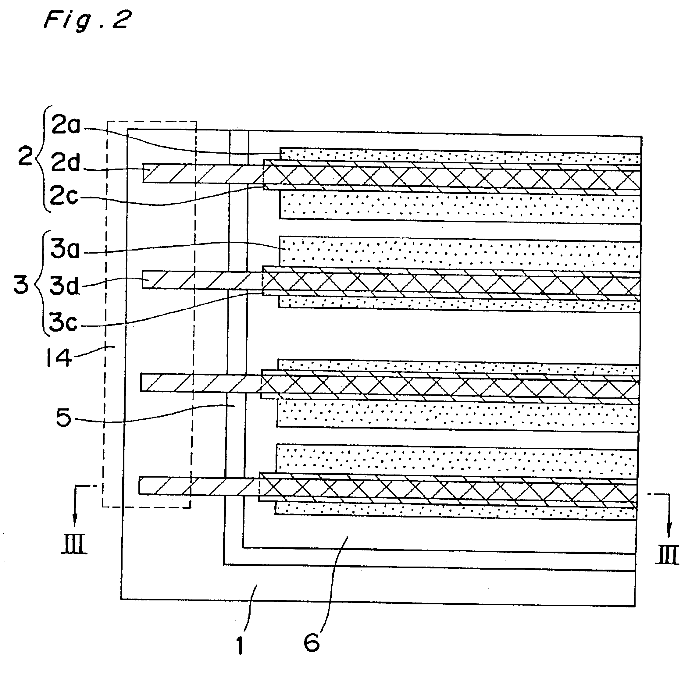
The plasma display panel has a configuration such that a front substrate 7 and rear substrates 13, are formed one upon another. The front substrate 7 includes a transparent first insulating substrate 1, a plurality of stripe-shaped first electrodes 4 extending parallel to each other, a dielectric layer 5, and a protection layer 6 formed in this order. The rear substrate 13 includes a second insulating substrate 8, a plurality of second electrodes 9 (called data electrodes in this embodiment) formed on the second insulating substrate 8 so as to extend parallel to each other, and a plurality of ribs 11 formed on the second insulating substrate 8 so as to separate neighboring (adjacent) second electrodes 9, forming a plurality of discharge spaces 10 therebetween. The plurality of first electrodes 4 extend generally perpendicular to the plurality o...

embodiment 2

FIG. 6 is a partially cutaway perspective view of a DC type plasma display panel according to the second embodiment of the present invention.

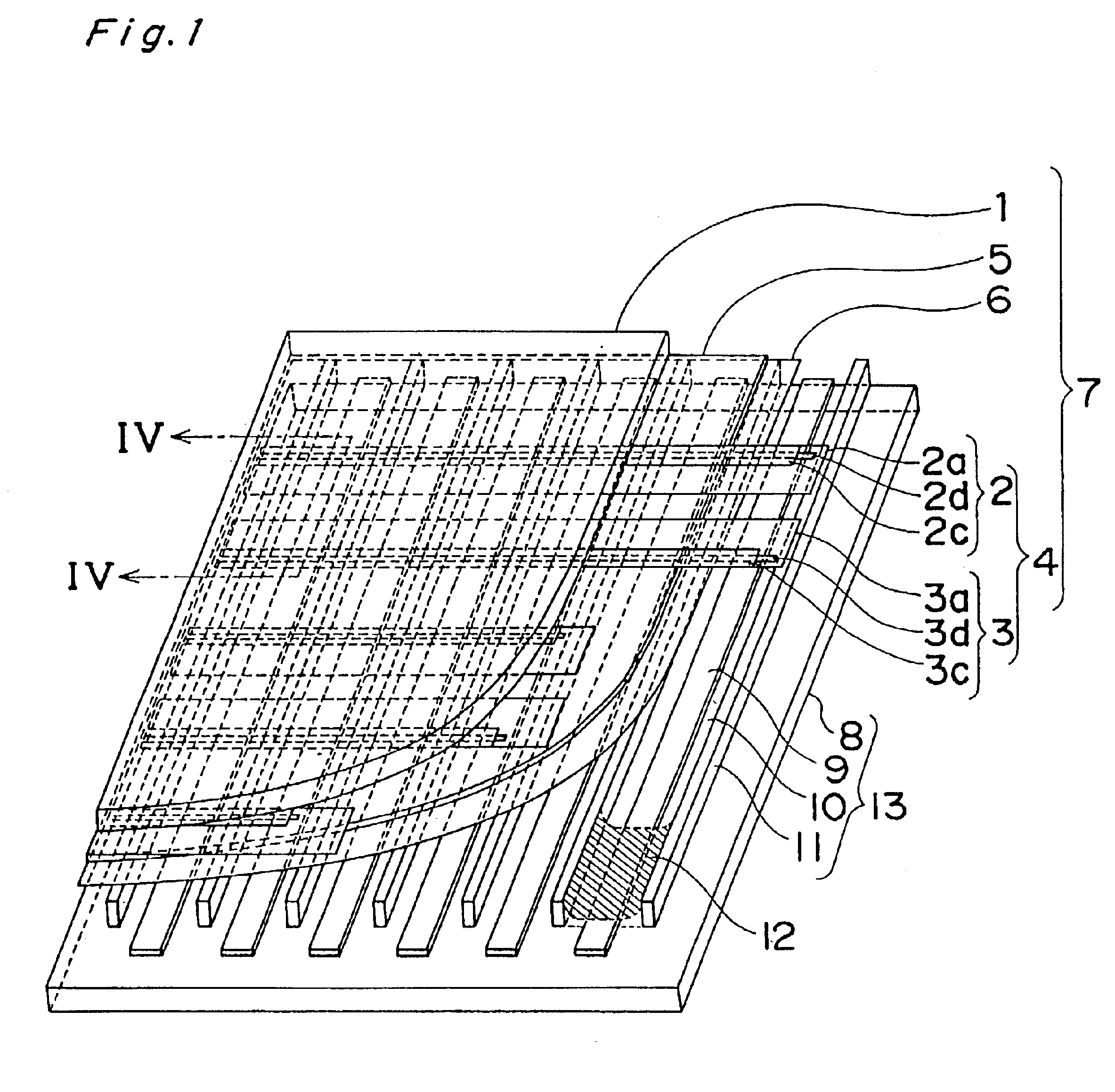
The plasma display panel has a configuration with a front substrate 16, including a first insulating substrate 1, and a plurality of first electrodes 15 disposed in parallel to each other as cathodes, and a rear substrate 13, including a plurality of stripe-shaped second electrodes 9 as anodes extending generally perpendicular to the plurality of first electrodes 15, and the stripe-shaped ribs 11 formed between the second electrodes 9 in parallel to each other and forming the discharge space 10, are formed one upon another. The first electrode 15 includes a discharge electrode constituted from a stripe-shaped black-colored -first conductive layer 15a and a second conductive layer 15b that is formed on the former and has a lower resistivity than the former.

The second conductive layer 15b is made with a width smaller than those of the first condu...


PUM


Abstract

A plasma display device having a front substrate and a rear substrate is provided. The front substrate is constituted from a transparent first insulating substrate, and a plurality of stripe-shaped first electrodes including at least one discharge electrode and extending parallel to each other. The rear substrate is constituted from a second insulating substrate, a plurality of second electrodes extending parallel to each other, and a plurality of ribs forming a plurality of discharge spaces therebetween. The discharge electrode includes a transparent electrode, a black-colored first conductive layer, and a second conductive layer. The second conductive layer has a lower resistivity than the first conductive layer and is made with widths smaller than those of the first conductive layer and extends to the edge of the first insulating substrate.

Description

BACKGROUND OF THE INVENTION1. Field of the InventionThe present invention relates to a plasma display panel used for displaying images of television, computer and other apparatuses.2. Description of Related ArtAn example of a plasma display panel of the prior art will be described below with reference to FIG. 7 which is a partially cutaway perspective view of an AC type plasma display panel.The plasma display panel is configured such that a front substrate includes a transparent first insulating substrate 51, a plurality of pairs of stripe-shaped scanning electrodes 52 and sustaining electrodes 53, a dielectric layer 54, and a protection layer 55 formed in this order. A rear substrate includes a second insulating substrate 56, a plurality of stripe-shaped data electrodes 57 extending perpendicular to the scanning electrodes 52 and the sustaining electrodes 53, and stripe-shaped ribs 59 formed on the second insulating substrate 56 forming a plurality of discharge spaces therebetween....

Claims


Application Information

Patent Timeline
Patent Type & Authority Patents(United States)
IPC IPC(8): H01J17/49H01J17/04H01J11/12H01J11/22H01J11/24H01J11/26H01J11/34H01J11/36H01J11/42H01J11/44H01J11/46
CPCH01J11/12H01J11/24H01J2211/444
Inventor FUJIWARA, SHINYA
Owner PANASONIC CORP
Why Eureka
Try Eureka