Inductance component and method of manufacturing the same

a technology of inductance components and manufacturing methods, applied in the field of inductance components, can solve the problems of inability to increase inductance, and achieve the effects of reducing undesirable magnetic effects on adjacent components, reducing inductance, and less magnetic flux leakag

Inactive Publication Date: 2005-03-08
PANASONIC CORP
View PDF7 Cites 22 Cited by
  • Summary
  • Abstract
  • Description
  • Claims
  • Application Information

AI Technical Summary

Benefits of technology

By the above configuration and manufacturing method, a magnetic material made of magnetic material is formed on the coil portion, and therefore, magnetic flux generated in the substrate due to the coil portion goes out of the substrate and passes through the magnetic material portion and again passes through the substrate, and thereby, a closed magnetic circuit loop is formed between the magnetic material portion and the substrate. Accordingly, it is possible to obtain an inductance component having increased inductance, less magnetic flux leakage, and reduced undesirable magnetic effects on adjacent components.

Problems solved by technology

Accordingly, inductance cannot be increased, and leaked magnetic flux causes undesirable magnetic effects to the adjacent components.

Method used


Image

  • Inductance component and method of manufacturing the same
  • Inductance component and method of manufacturing the same
  • Inductance component and method of manufacturing the same

Examples


first preferred embodiment

The first preferred embodiment will be described in the following with reference to the drawings.

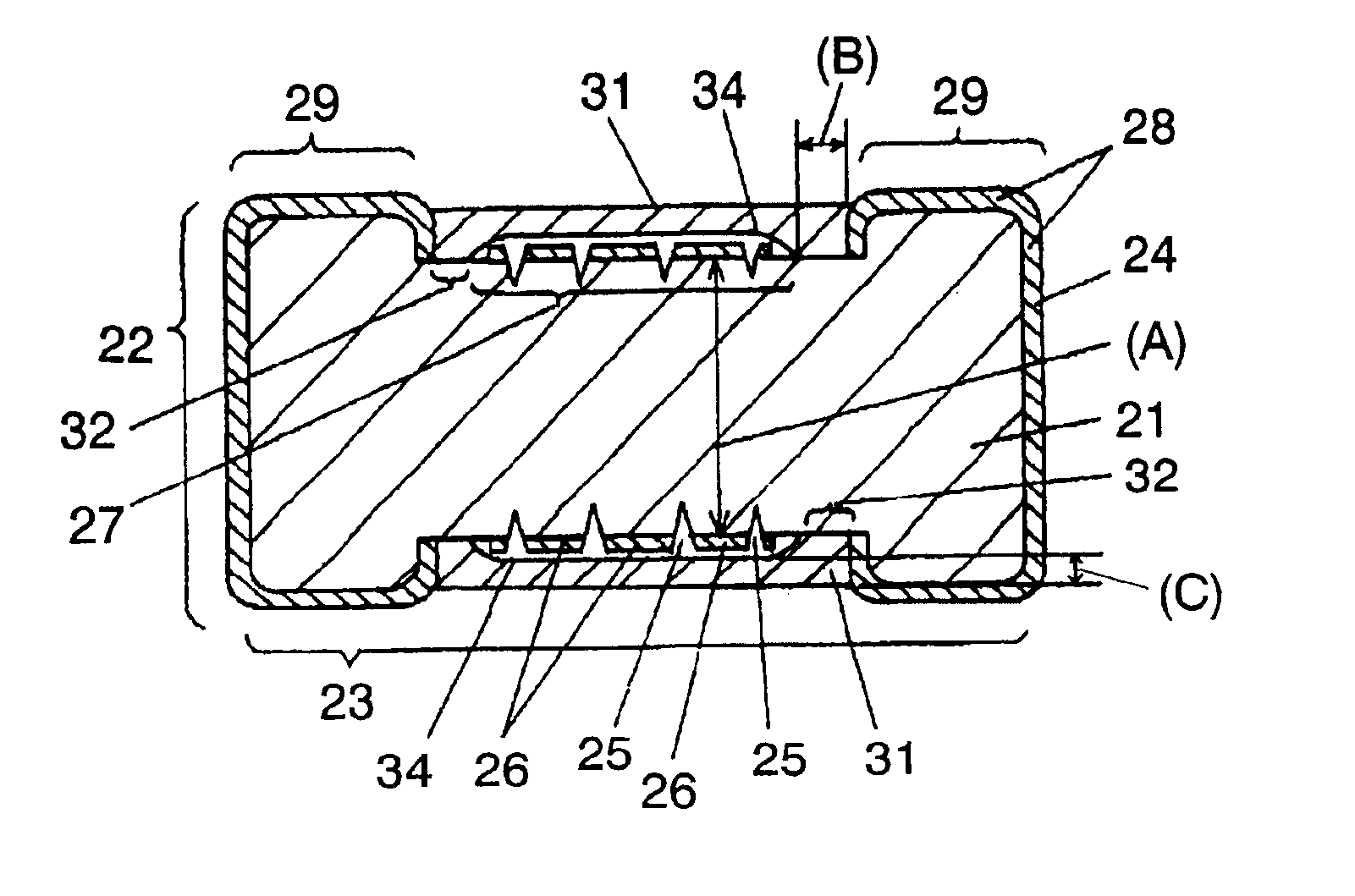
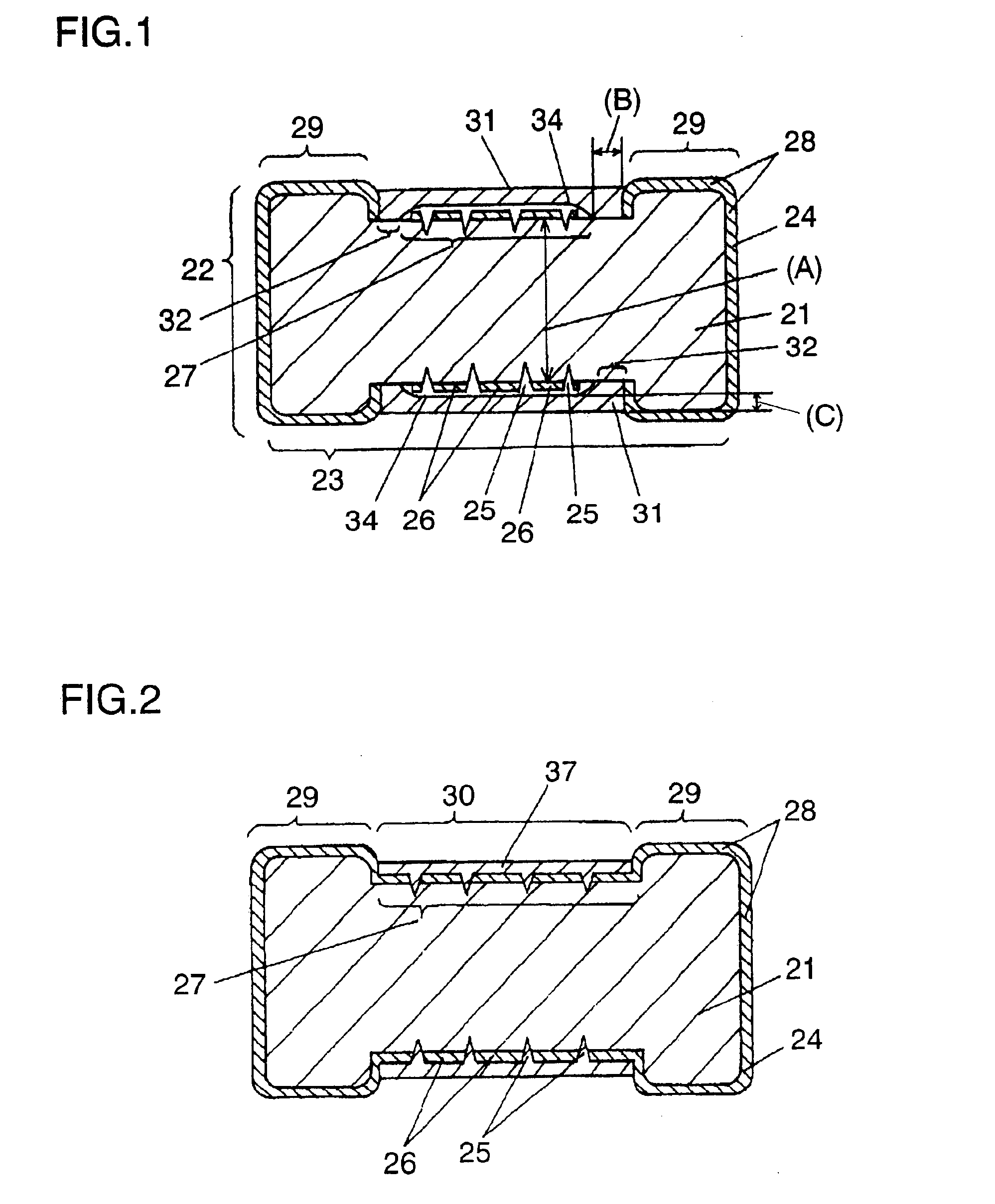
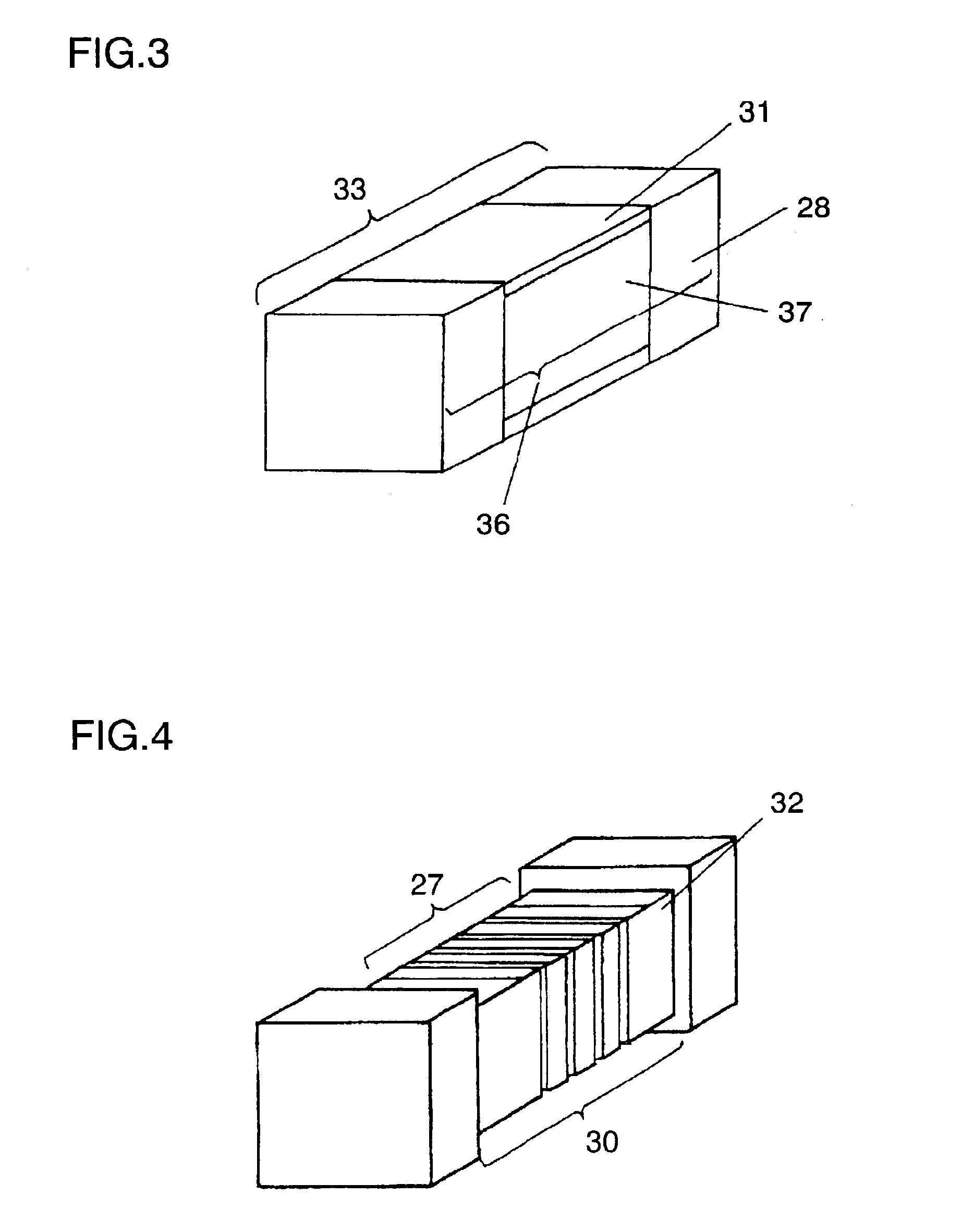
In FIG. 1-FIG. 4, an inductance component in the first preferred embodiment of the present invention comprises a column-shaped substrate 21 made of magnetic material, a conductor layer 24 covering the end surfaces 22 and peripheral surface 23 of the substrate 21, a coil portion 27 having a groove portion 25 and wire conductor portion 26, formed by spirally cutting the conductor layer 24 by a laser beam, and an electrode portion 28 formed of the conductor layer 24 covering both end portions 29 of the substrate 21. The substrate 21 is, as shown in FIG. 2, provided with a recess 30 between the end portions 29, and the coil portion 27 is disposed in the recess 30.

Also, there is provided a magnetic material portion 31 made of a magnetic material on the coil portion 27. The magnetic material portion 31 is a sintered magnetic material formed by sintering magnetic material, and the conductor lay...

second preferred embodiment

The second preferred embodiment will be described in the following with reference to the drawings.

The inductance component in the second preferred embodiment of the present invention is an improved version of the inductance component in the first preferred embodiment of the present invention.

In FIG. 8 to FIG. 11, the inductance component in the second referred embodiment of the present invention comprises a parallelepiped column shaped substrate 21 made of magnetic material, a conductor layer 24 covering the end surface 22 and peripheral surface 23 of the substrate 21, a coil portion 27 having groove portion 25 and wire conductor portion 26, formed by spirally cutting the conductor layer 24 covering the peripheral surface 23 of the substrate 21, and an electrode portion 28 of the conductor layer 24 covering each end portion 29 of the substrate 21.

Also, on the coil portion 27 is disposed a magnetic material portion 31 made of magnetic material, and the magnetic material portion 31 is...


PUM

PropertyMeasurementUnit
thickaaaaaaaaaa
inductanceaaaaaaaaaa
magneticaaaaaaaaaa

Abstract

An inductance component comprising a column-shaped magnetic material substrate 21, conductor layer 24 covering ends and a peripheral surface of the substrate, coil portion 27 having groove portion 25 and wire conductor portion 26 formed in the conductor layer covering the peripheral surface, electrode portions 28 including the conductor layer covering the ends of the substrate, and magnetic material portion 31 made of sintered magnetic material on the coil portion, wherein the conductor layer has a melting point higher than a sintering temperature of the sintered magnetic material. The manufacturing process comprises forming a substrate, forming a conductor layer, forming a coil portion, forming electrode portions at ends of the substrate, and forming a magnetic material portion of sintered magnetic material on the coil portion. The present invention provides an inductance component with high inductance, low magnetic flux leakage, and less undesirable magnetic effects on adjacent components.

Description

TECHNICAL FIELDThe present invention relates to an inductance component used in electronic equipment, communication equipment and the like, and a method of manufacturing the same.BACKGROUND ARTA conventional inductance component is described in the following with reference to the drawings.FIG. 16 is a sectional view of a conventional inductance component, and FIG. 17 is a perspective view of a substrate of the inductance component.In FIG. 16 and FIG. 17, a conventional inductance component comprises a column-shaped substrate 11 made of insulating material, a conductor layer 12 covering the substrate 11, a groove portion 13 formed by cutting the conductor layer 12, a coil portion 14 formed by spirally cutting the groove portion 13, electrodes 16 disposed at both end of the substrate 11, and a covering portion 15 made of insulating resin covering the coil portion 14.Also, the substrate 11 has steps 17 between the ends thereof, forming a recess 18, as shown in FIG. 17, and the coil por...

Claims


Application Information

Patent Timeline
Patent Type & Authority Patents(United States)
IPC IPC(8): H01F41/04H01F17/04
CPCH01F41/046H01F17/045H01F17/0033H01F41/04
Inventor KANETAKA, TOYONORIYOSHIZAWA, TOSHIHIROYAMAMOTO, HIROMASA
Owner PANASONIC CORP
Why Eureka
Try Eureka