
Memory circuit with redundant configuration

a memory circuit and configuration technology, applied in the field of memory circuits with redundant configurations, can solve the problems of word line and sector errors, drop in access speed, drop in yield, etc., and achieve the effect of preventing the drop in access speed due to redundancy judgmen

Active Publication Date: 2005-03-08
INFINEON TECH LLC
View PDF3 Cites 25 Cited by
  • Summary
  • Abstract
  • Description
  • Claims
  • Application Information

AI Technical Summary

Benefits of technology

With the foregoing in view, it is an object of the present invention to provide a memory circuit where a drop in access speed due to redundancy judgment is prevented.
It is another object of the present invention to provide a memory circuit which enables an operation test of the spare sectors and repaired regular sectors regardless the redundant address.
In the above aspect of the present invention, it is preferable that a word line decoder for selecting a word line in the sector is disposed in each sector, and the input signal of the word line decoder is supplied to the first and second blocks. In other words, the input signal of the word line decoder is supplied to the first block selected by the supplied address and the second block, which is a pair of the first block. This makes it possible to select a word line by the word line decoder in the regular sector and to select a word line by the word line decoder in the spare sector, which are selected simultaneously.
Also in a preferred embodiment, a Y gate circuit for selecting a bit line in a block is disposed in each block, and a bit line in the first block is selected when the result of redundancy judgment is a mismatch, and a bit line in the second block is selected when the result of redundancy judgment is a match. And it is preferable that both of these bit lines are never selected simultaneously while the regular sector and the spare sector are simultaneously selected during the first period. By this, contention of both of these bit lines via a common data bus line can be prevented.
In the above embodiment, it is preferable that a Y gate select signal to be supplied to a Y gate circuit starts to be driven according to the result of redundancy judgment before the first period ends. Since the timing of the result of redundancy judgment by a redundancy judgment circuit disperses, the first period is set during which the regular sector and the spare sector thereof are simultaneously selected. As a result, the Y gate is selected by either the first or second block. Therefore selection of the Y gate may be switched depending on the result of redundancy judgment. By switching the selection of the Y gate, the boost power supply level for sharing power supply with the Y gate select signal drops. In the preferred embodiment, delay of recovery of the column boost power supply which supplies power of the Y gate select signal can be prevented by driving the Y gate select signal before ending the first period.

Problems solved by technology

In this kind of flash memory, defects of word lines and sectors, which are the units of erasing, are becoming a major cause of a drop in yield, due to increasing capacity.
A drop in access speed is the problem in such a memory with a redundant configuration.
Therefore selection start timing at the spare sector side delays for the amount of time required for comparison judgment with the redundant address.

Method used


Image

  • Memory circuit with redundant configuration
  • Memory circuit with redundant configuration
  • Memory circuit with redundant configuration

Examples


second embodiment

[Second Embodiment]

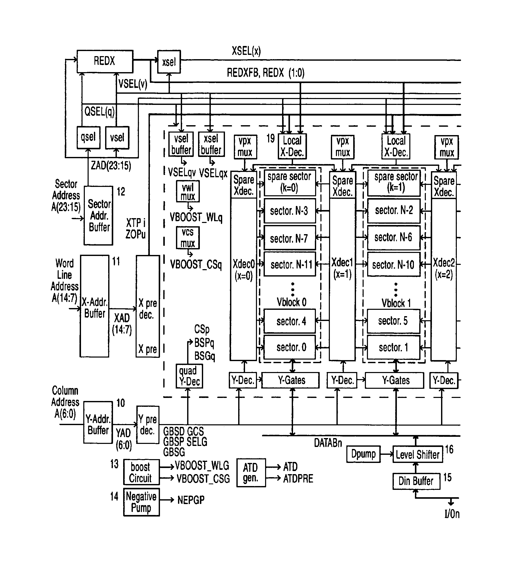
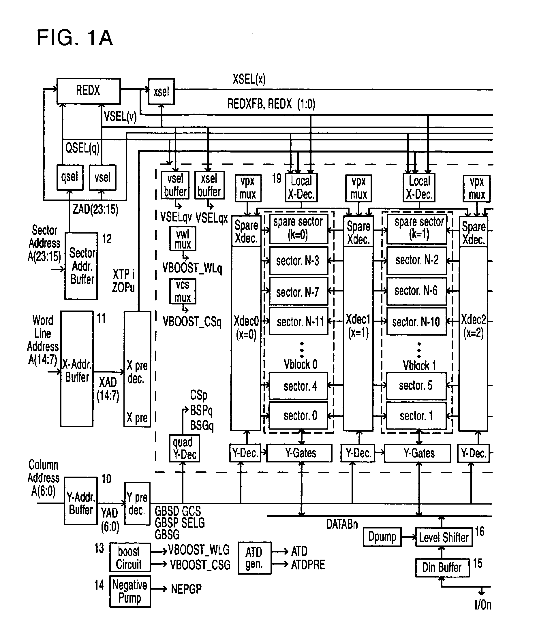
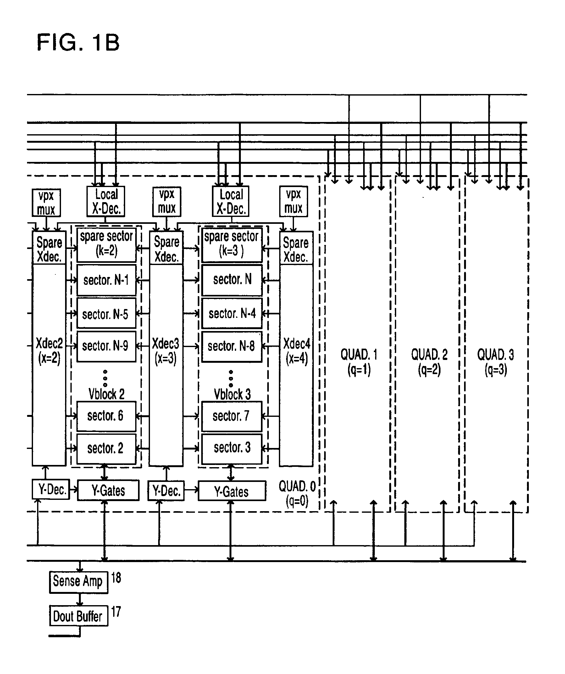
The second embodiment will now be described. The memory circuit of this embodiment also comprises a plurality of regular sectors and spare sectors, as shown in FIGS. 1, 2 and 3, and further comprises a redundancy judgment circuit REDX, as shown in FIG. 9. And responding to the test signal TEST, which is a first signal, the redundancy judgment circuit REDX sets the redundancy judgment signal REDXFB to a match status, regardless the address in the redundant memory, and enables access to the spare sector. For this the AND gates 34, 36 and 38 are disposed. Therefore other judgment signals REDX(0), (1) are also forcibly set to match status, and the simultaneous erase mode disable signal DISFCERB is also forcibly set to a match status (disable status).

Also responding to the redundancy disable signal DISRED, which is a second signal, the redundancy judgment circuit REDX sets the redundancy judgment signal REDXFB to a mismatch status regardless the address in the redundan...


PUM


Abstract

A memory circuit has a plurality of blocks which further comprises a plurality of regular sectors and a spare sector, wherein each sector further comprises a plurality of memory cells, and when a regular sector in a first block is defective, this defective regular sector is replaced with a spare sector in a second block. And responding to an address to be supplied, the regular sector corresponding to the supplied address in the first block and the spare selector in the second block are selected simultaneously during a first period, and after the first period, selection of one of the regular sector and the spare sector is maintained according to the result of redundancy judgment on whether the supply address matches with the redundant address. Regardless the result of redundancy judgment on whether the supplied address matches the redundant address indicating the defective sector, a regular sector in the first block and the spare sector in the second block, to be a pair thereof, are set to selected status simultaneously during the first period when access operation stars, so a drop in access speed due to a redundancy judgment operation can be suppressed.

Description

CROSS-REFERENCE TO RELATED APPLICATIONSThis application is based upon and claims the benefit of priority from the prior Japanese Patent Application No. 2002-265065, filed on Sep. 11, 2002, the entire contents of which are incorporated herein by reference.BACKGROUND OF THE INVENTION1. Field of the InventionThe present invention relates to a memory circuit with a redundant configuration, and more particularly to a memory circuit where a drop in access speed due to redundancy judgment is prevented.2. Description of the Related ArtA semiconductor memory device has a redundant configuration for repairing defective cells which are generated due to miniaturization as capacity increases and other causes. Various redundant configurations are used for such semiconductor memories as DRAM, SRAM, FeRAM and EEPROM (flash memory). Of these, flash memory uses a redundant configuration of bit lines as a repair method of defective cells. In other words, a bit line to which a defective cell belongs is...

Claims


Application Information

Patent Timeline
IPC IPC(8): G11C29/24G11C29/00G11C29/04G11C16/02G11C16/06
CPCG11C29/24G11C29/846G11C29/82G11C29/00
Inventor TSUKIDATE, YOSHIHIROKURIHARA, KAZUHIROKASA, YASUSHINAKAI, TSUTOMUCHEUNG, ANDY
Owner INFINEON TECH LLC
Learn More