
Substrate for electrooptical device, method for manufacturing the substrate, electrooptical device, method for manufacturing the electrooptical device, and electronic apparatus

a technology of electrooptical devices and substrates, applied in non-linear optics, identification means, instruments, etc., can solve the problems of unsatisfactory conditions for rubbing process of alignment films, non-uniform gap, and inability to clearly see the image of the display, so as to achieve the effect of reducing the dispersion of the cell gap

Inactive Publication Date: 2005-03-15
BOE TECH GRP CO LTD
View PDF3 Cites 7 Cited by
  • Summary
  • Abstract
  • Description
  • Claims
  • Application Information

AI Technical Summary

Benefits of technology

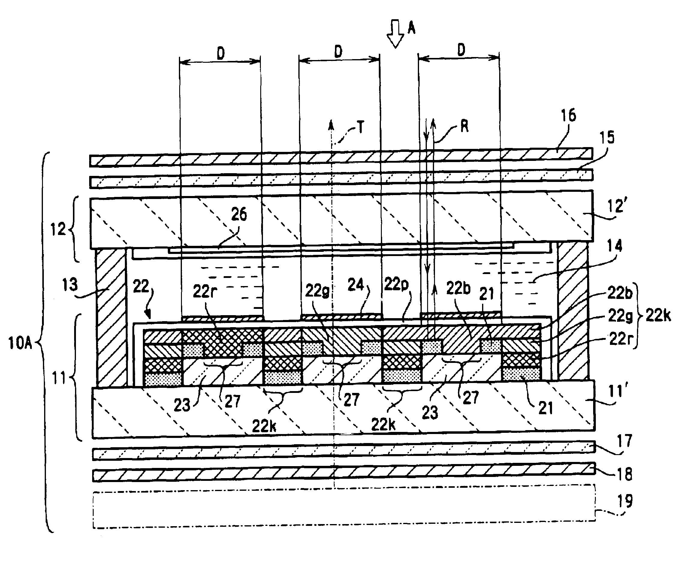
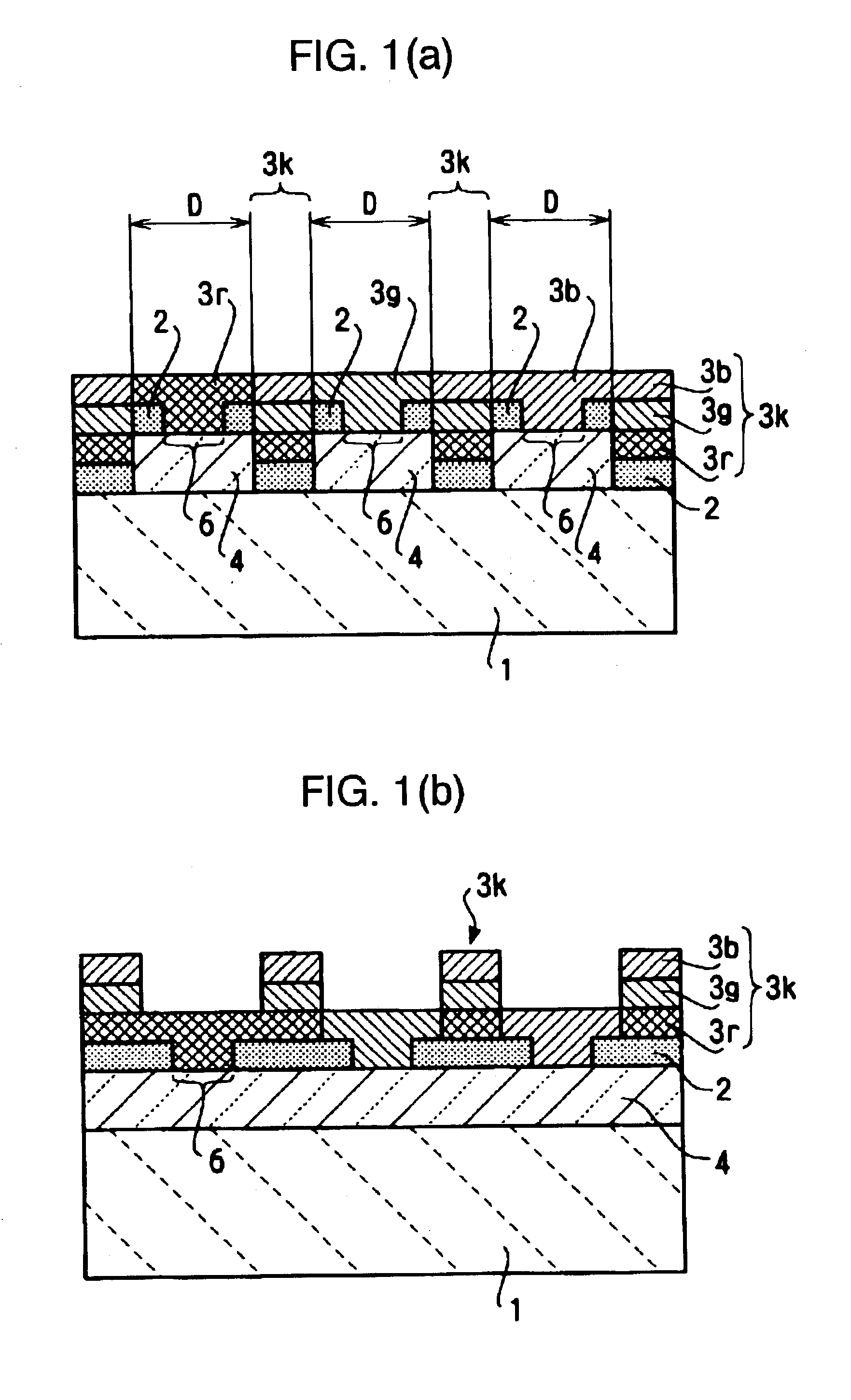
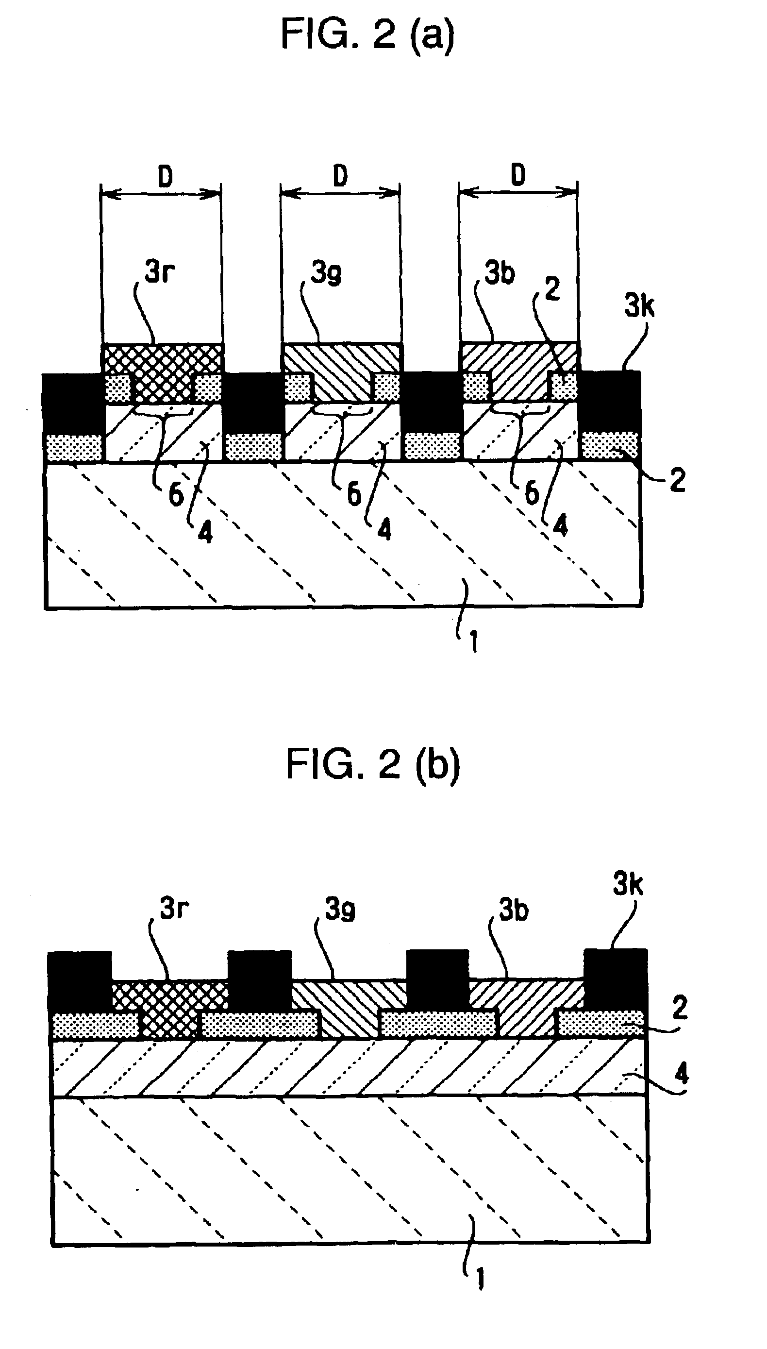
Since the underlayer is not provided at the regions between the display dots, that is, since the underlayer is not provided at the regions where the light-shielding layer is formed, the thickness at a part where the light-shielding layer is formed is reduced by an amount corresponding to the thickness of the underlayer. Accordingly, the light-shielding layer can be prevented from projecting from the surface, so that the roughness of the substrate surface can be reduced. More specifically, the planarity of the substrate surface can be improved.
In addition, in the above-described method for manufacturing the electrooptical device, the light-shielding layer is preferably formed such that the height of the light-shielding layer is approximately the same as the height of the underlayer. In such a case, the light-shielding layer and the underlayer are leveled with respect to the base plate, so that the planarity over the surfaces of the display dots and the surfaces of the boundary regions between the display dots can be ensured and the dispersion of the cell gap becomes smaller.

Problems solved by technology

Meanwhile, in a liquid crystal device which can perform reflective display, irrespective of whether it is a transflective liquid crystal device or a reflective liquid crystal device, there is a problem in that when the surface of the reflective layer is mirror-finished, a displayed image cannot be seen clearly by a viewer due to the reflection of objects and room lights on the image.
Accordingly, there are problems in that a cell gap becomes nonuniform and a rubbing process of an alignment film cannot be performed under satisfactory conditions.
Although a substrate surface becomes relatively planar when an alignment layer and an overcoat layer are generally formed on the light-shielding layer, the above-described problems of nonuniform cell gap, etc., cannot be solved.

Method used


Image

  • Substrate for electrooptical device, method for manufacturing the substrate, electrooptical device, method for manufacturing the electrooptical device, and electronic apparatus
  • Substrate for electrooptical device, method for manufacturing the substrate, electrooptical device, method for manufacturing the electrooptical device, and electronic apparatus
  • Substrate for electrooptical device, method for manufacturing the substrate, electrooptical device, method for manufacturing the electrooptical device, and electronic apparatus

Examples


seventh embodiment

Next, another embodiment in which the present invention is applied to a transflective passive-matrix liquid crystal device will be described. FIG. 34 is a sectional view of a liquid crystal panel included in the liquid crystal device according to another embodiment of the present invention. FIG. 35 is a sectional view of a color filter substrate included in the liquid crystal panel shown in FIG. 34. FIG. 36 is an enlarged view of a part of the liquid crystal panel. FIG. 34 corresponds to a sectional view of FIG. 36 cut along line A-A′. FIG. 37 is an enlarged sectional view of a part of a light-shielding layer from which a resin scattering layer is completely removed. FIG. 38 is an enlarged sectional view of a part of the light-shielding layer from which the resin scattering layer is partially removed. FIG. 39 is a flow chart showing a method for manufacturing the liquid crystal device according to the present embodiment.

A liquid crystal panel 502 shown in FIG. 34 is a transflective ...

eighth embodiment

Next, another embodiment in which the present invention is applied to a transflective passive-matrix liquid crystal device will be described. FIG. 40 is a sectional view of a liquid crystal panel included in the liquid crystal device according to another embodiment of the present invention. FIG. 41 is a sectional view of a color filter substrate included in the liquid crystal panel shown in FIG. 40. FIG. 42 is an enlarged view of a part of the liquid crystal panel. FIG. 40 corresponds to a sectional view of FIG. 42 cut along line A-A′. FIG. 43 is an enlarged sectional view of a part of a light-shielding layer from which an underlayer is completely removed. FIG. 44 is an enlarged sectional view of a part of the light-shielding layer from which the underlayer is partially removed. FIG. 45 is a flow chart showing a method for manufacturing the liquid crystal device according to the present embodiment.

A liquid crystal panel 602 shown in FIG. 40 is a transflective liquid crystal panel, a...

ninth embodiment

Next, another embodiment in which the present invention is applied to a transflective liquid crystal device using Thin Film Diodes (TFD), which are two-terminal switching devices, as switching devices will be described below.

FIG. 46 is a sectional view of a part including a first base plate included in a liquid crystal device according to another embodiment of the present invention. FIG. 47 is a sectional view of a part including a first base plate included in the liquid crystal panel shown in FIG. 46. FIG. 48 is an enlarged view of a part of the liquid crystal panel. FIG. 46 corresponds to a sectional view of FIG. 48 cut along lines B-B′ and C-C′. FIG. 49 is an enlarged sectional view of a part of a light-shielding layer from which an underlayer is completely removed. FIG. 50 is an enlarged sectional view of a part of the light-shielding layer from which the underlayer is partially removed. FIG. 51 is a flow chart showing a method for manufacturing the liquid crystal device accordi...


PUM

PropertyMeasurementUnit
thicknessaaaaaaaaaa
thicknessaaaaaaaaaa
thicknessaaaaaaaaaa

Abstract

A substrate for an electrooptical device includes a base 1 having a plurality of display dots D, an underlayer 4 formed on the base 1, a reflective layer 2 formed on the underlayer 4, and color layers 3r, 3g, and 3b formed on the reflective layer 2. The underlayer 4 is provided at regions corresponding to the display dots D, but is not provided at regions between the display dots D. In addition, concave areas are provided at regions between the display dots D, and a light-shielding layer 3k is provided to fill the concave areas. Accordingly, the light-shielding layer 3k, and the-color layers 3r, 3g, and 3b are level with each other.

Description

TECHNICAL FIELDThe present invention relates to a substrate used in an electrooptical device such as a liquid crystal device, a method for manufacturing the substrate, an electrooptical device including the substrate, and an electronic apparatus including the electrooptical device.BACKGROUND ARTRecently, electrooptical devices have been commonly used in electronic apparatuses such as cellular phones and portable personal computers. Transflective liquid crystal devices, which can perform both reflective display and transmissive display, are known as one of such electrooptical devices.When a transflective liquid crystal device performs reflective display, external light such as natural light and room light enters the liquid crystal device and is reflected by a reflective layer provided in the liquid crystal device. Thus, an image is displayed when the reflected light is emitted to the outside. The reflective layer must also have a function to transmit light so that the liquid crystal ...

Claims


Application Information

Patent Timeline
Patent Type & Authority Patents(United States)
IPC IPC(8): G02F1/1335G02F1/13G02F1/1333G09F9/30
CPCG02F1/133512G02F2203/02G02F2201/48G02F1/1333
Inventor TAKIZAWA, KEIJIOTAGIRI, YOSHIHIRONAKANO, TOMOYUKIKANEKO, HIDEKIMATSUO, MUTSUMIOTAKE, TOSHIHIRO
Owner BOE TECH GRP CO LTD
Learn More