Integrated circuit device

a circuit device and integrated circuit technology, applied in the field of integrated circuit devices, can solve the problems of obstructing software processing, affecting the execution time of programs, and merely affecting the execution time of cache memory, so as to improve processing efficiency, and reduce the number of surplus circuit elements

Inactive Publication Date: 2005-03-15
FUJIFILM BUSINESS INNOVATION CORP
View PDF7 Cites 26 Cited by
  • Summary
  • Abstract
  • Description
  • Claims
  • Application Information

AI Technical Summary

Benefits of technology

This is to say, an integrated circuit device according to the present invention includes a first memory for inputting data into and / or outputting data from a second memory and a processing unit in which at least one data flow is formed and at least part of at least one data flow is changeable, the processing unit including a data processing section that processes data that is inputted from and / or outputted to the first memory, a first address outputting section that outputs a first address of data that is inputted and / or outputted between the first memory and the data processing section, and a second address outputting section that outputs a second address of data that is inputted and / or outputted between the first memory and the second memory. By constructing a first address outputting section and a second address outputting section using part of the processing unit where the data flows can be changed, using the hardware configuration of the data processing section or the software executed in the data processing section, it is possible to change the data flow of the first address outputting section or the second address outputting section and to control the outputs of these sections. Accordingly, a cache system that is optimal for the processing executed by an integrated circuit device can be configured in the integrated circuit device. Alternatively, it is possible to configure a control circuit for a cache memory in the integrated circuit device so that a cache system can be optimally controlled for the processing executed by the integrated circuit device.
By incorporating a code memory for storing program code that has the control unit perform the above processing, it becomes possible to construct an integrated circuit device, such as a single-chip system LSI. Accordingly, it becomes possible to provide integrated circuit devices with improved execution speed where a cache or cashes are used efficiently for a variety of types of software without causing overheads. It is also possible to provide a processing unit whose data flows can be reconfigured as a separate chip, as a processor core, or as a chip in which the first memory used as the cache memory is also incorporated. In this way, the present invention can be embodied in a variety of ways, with processing devices that correspond to such embodiments also being included within the scope of the present invention.

Problems solved by technology

When the hit rate of the cache memory is low, the cache memory becomes merely an overhead that detrimentally affects the execution time of programs.
However, when applying the cache that is separated into an instruction cache and a data cache, if instructions and data are simultaneously present in one block, it becomes difficult to handle the instructions and the data.
For example, rewriting instructions may cause obstruct to software processing.
Also, in software where instructions and data are not accessed equally, there is no improvement in efficiency by simply separating the cache.
For example, when the accesses to data are sporadic, the usage efficiency of the data cache is low, so that there is the possibility of this becoming an overhead.
However, when the cache is constructed hierarchically, there is an inevitable rise in the number of accesses to the memory, so that there is always the possibility of overheads depending on conditions such as the structure of the software and the input / output media for the data being processed.
Even when prefetching is performed, penalties due to branch instructions or the like cannot be avoided.
However, since cache memory is hardware that is disposed in an intermediate position between the CPU and the external memory, when there are differences in the processing content of the software to be executed or in the hardware environment that stores the data to be processed by this software, this can cause problems such as the predicted cache efficiency not being obtained and conversely in overheads being produced, which increases the execution time of the processor.

Method used


Image

  • Integrated circuit device
  • Integrated circuit device
  • Integrated circuit device

Examples


Embodiment Construction

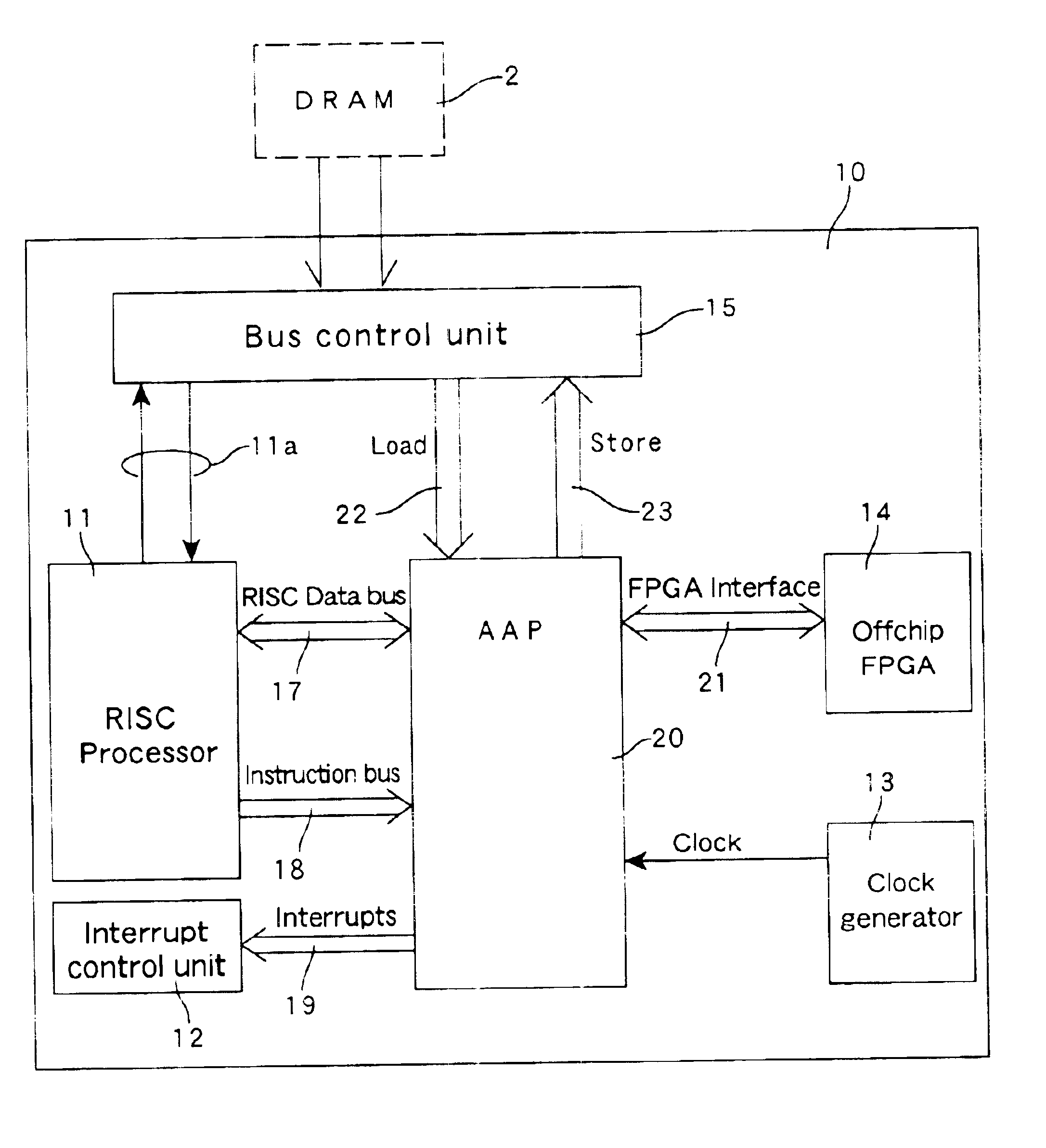
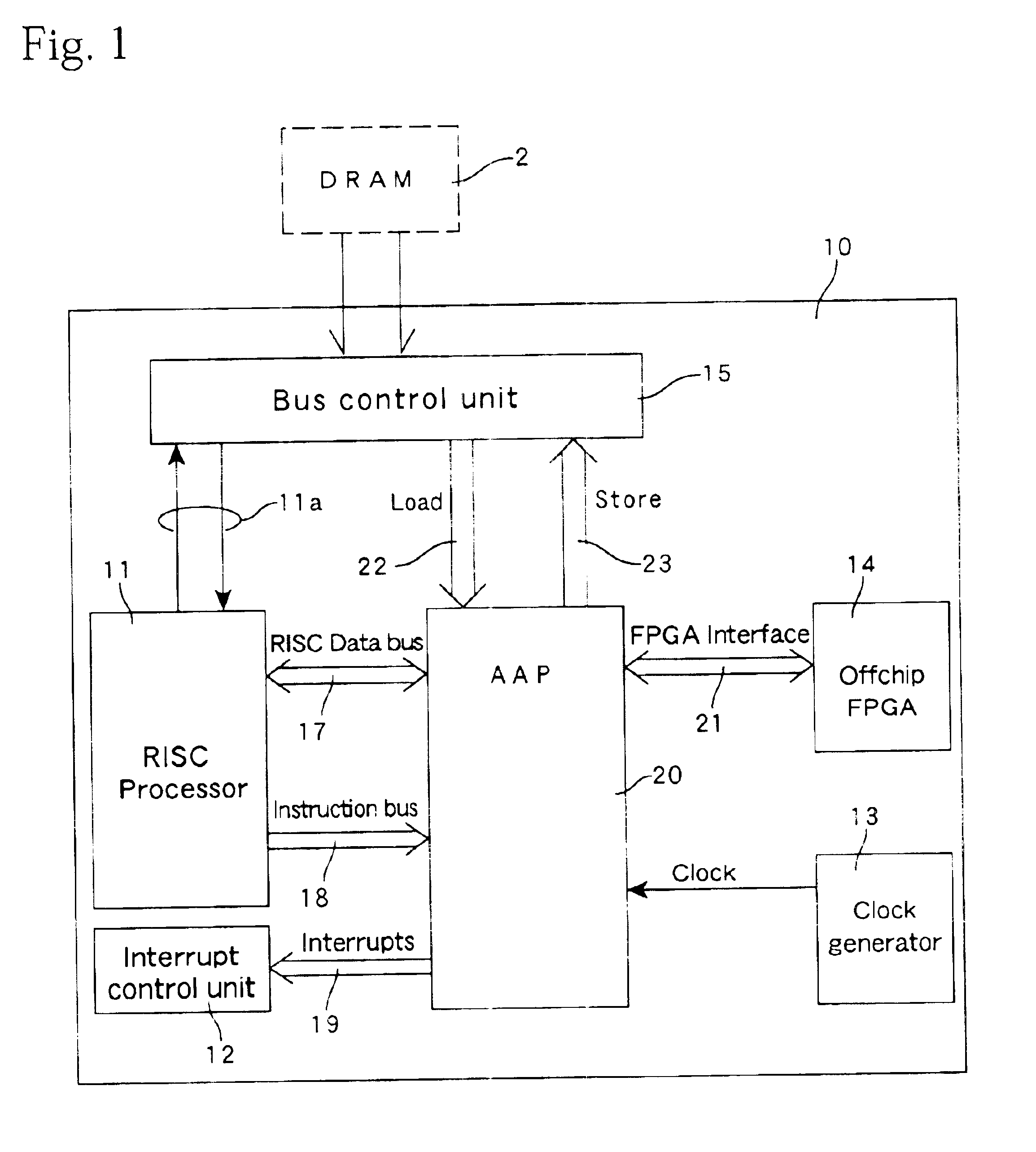
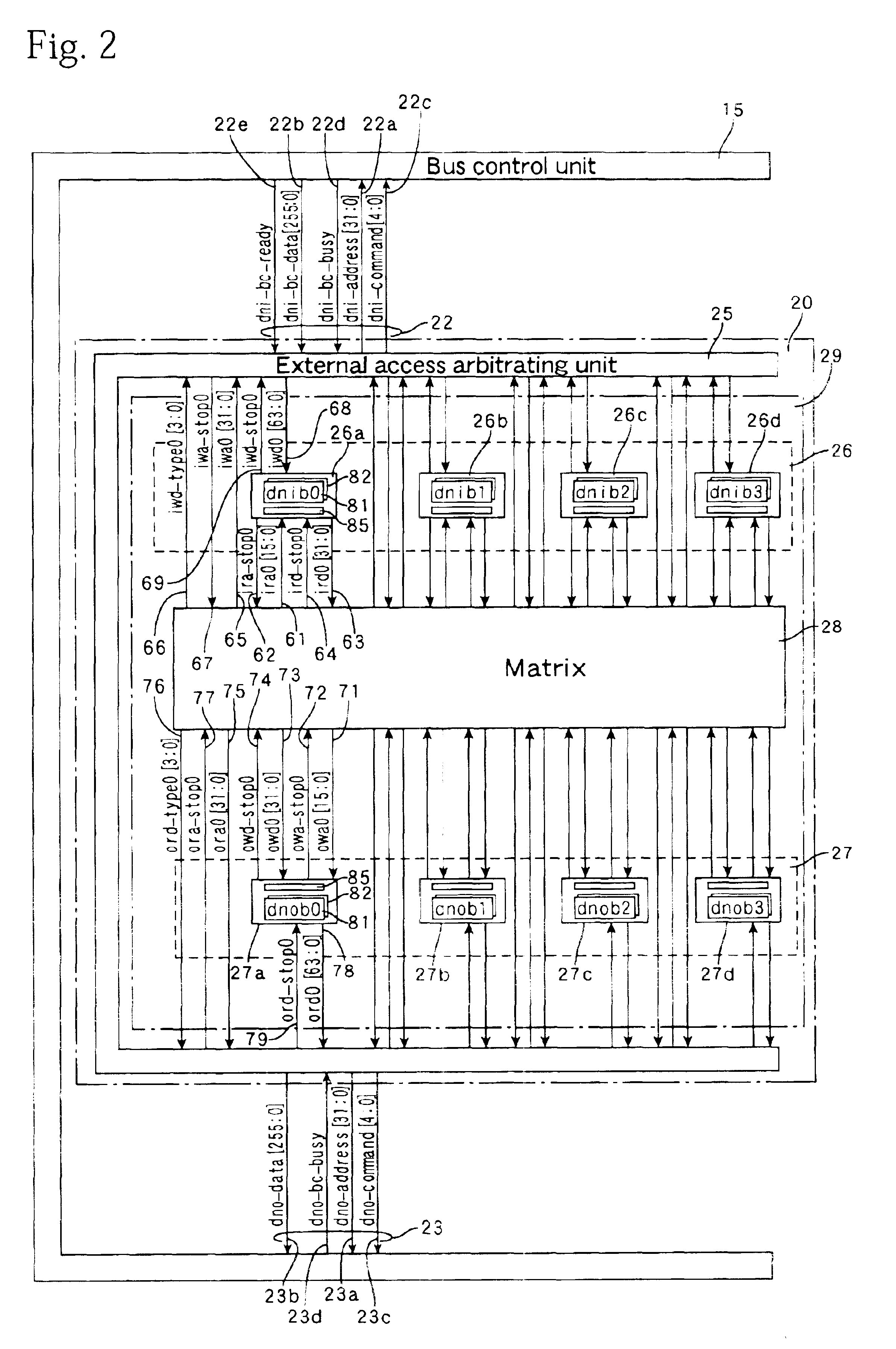
The following describes the present invention with reference to the attached drawings. FIG. 1 shows the outline configuration of a system LSI 10 according to the present invention. This LSI 10 is a data processing system that includes a processor unit 11, an AAP (Adoptive Application Processor) portion or unit (hereinafter AAP) 20, an interrupt control unit 12, a clock generating unit 13, an FPGA unit 14, and a bus control unit 15. The processor unit 11 (hereinafter “basic processor” or “processor”) that has a general-purpose construction and performs general purpose processing, including error handling, based on instruction sets that are provided by a program or the like. In the AAP unit 20, data flows or virtual data flows that are suited to special-purpose data processing are variably formed by a plurality of operation or logical elements that are arranged in a matrix. The interrupt control unit 12 controls interrupt handling for interrupts from the AAP 20. The clock generating u...


PUM


Abstract

In an integrated circuit device that includes a first memory that is capable of inputting data into and / or outputting data from a second memory and a processing unit in which at least part of at least one data flow is changeable, the processing unit includes, in addition to a data processing section that processes data that is inputted from and / or outputted to the first memory, a first address outputting section that outputs a first address of data that is inputted and / or outputted between the first memory and the data processing section and a second address outputting section that outputs a second address of data that is inputted and / or outputted between the first memory and the second memory. By using part of the processing unit, where a data flow can be changed or reconfigured, for configuring a circuit that controls the memories, a cache memory system that is optimal for the processing executed by the integrated circuit device can be configured in the integrated circuit device.

Description

TECHNICAL FIELDThe present invention relates to an integrated circuit device in which data flows can be reconfigured.RELATED ARTWhen data and / or instructions (hereinafter referred to as “data” where there is no particular need to distinguish between “instructions” and “data”), which are stored in a memory, such as a RAM, a ROM, or a magnetic disc, are processed by a CPU or the like, a high speed memory called a “cache” or “cache memory” that has a comparatively small capacity is used and the access speed for the data is improved by utilizing the temporal locality and / or spatially locality of the data. Accordingly, in an integrated circuit device such as a VLSI, a system LSI, or a system ASIC where a processor or a processor core is incorporated, a cache system comprising a cache memory and an MMU (Memory Management Unit) for controlling the cache memory is also incorporated.When a cache memory is used, an MMU and a TLB (Translation Look-Aside Buffer) are used, so that when the data ...

Claims


Application Information

Patent Timeline
Patent Type & Authority Patents(United States)
IPC IPC(8): G06F15/78G06F15/76
CPCG06F15/7867G06F15/7846G06F15/781G06F3/00
Inventor IKEDA, KENJI
Owner FUJIFILM BUSINESS INNOVATION CORP
Why Eureka
Try Eureka