High density mask ROM having flat-type bank select

a high-density, mask-type technology, applied in static storage, digital storage, instruments, etc., can solve the problems of affecting the overall size of the array, affecting the layout area, and the contact size and metal pitch become the limit, so as to reduce the effect of metal coupling, reduce the number of contacts and transistors, and increase cell curren

Inactive Publication Date: 2005-03-22
MACRONIX INT CO LTD
View PDF6 Cites 0 Cited by
  • Summary
  • Abstract
  • Description
  • Claims
  • Application Information

AI Technical Summary

Benefits of technology

It is one object of the present invention to provide an architecture of a flat-type ROM. The contact and transist

Problems solved by technology

While the memory cell is shrinking down, the contact size and metal pitch become the limit of it.
On the other hand, memory array used to use LOCOS-type MOS for the bank selection transistors, which ca

Method used


Image

  • High density mask ROM having flat-type bank select
  • High density mask ROM having flat-type bank select
  • High density mask ROM having flat-type bank select

Examples


first embodiment

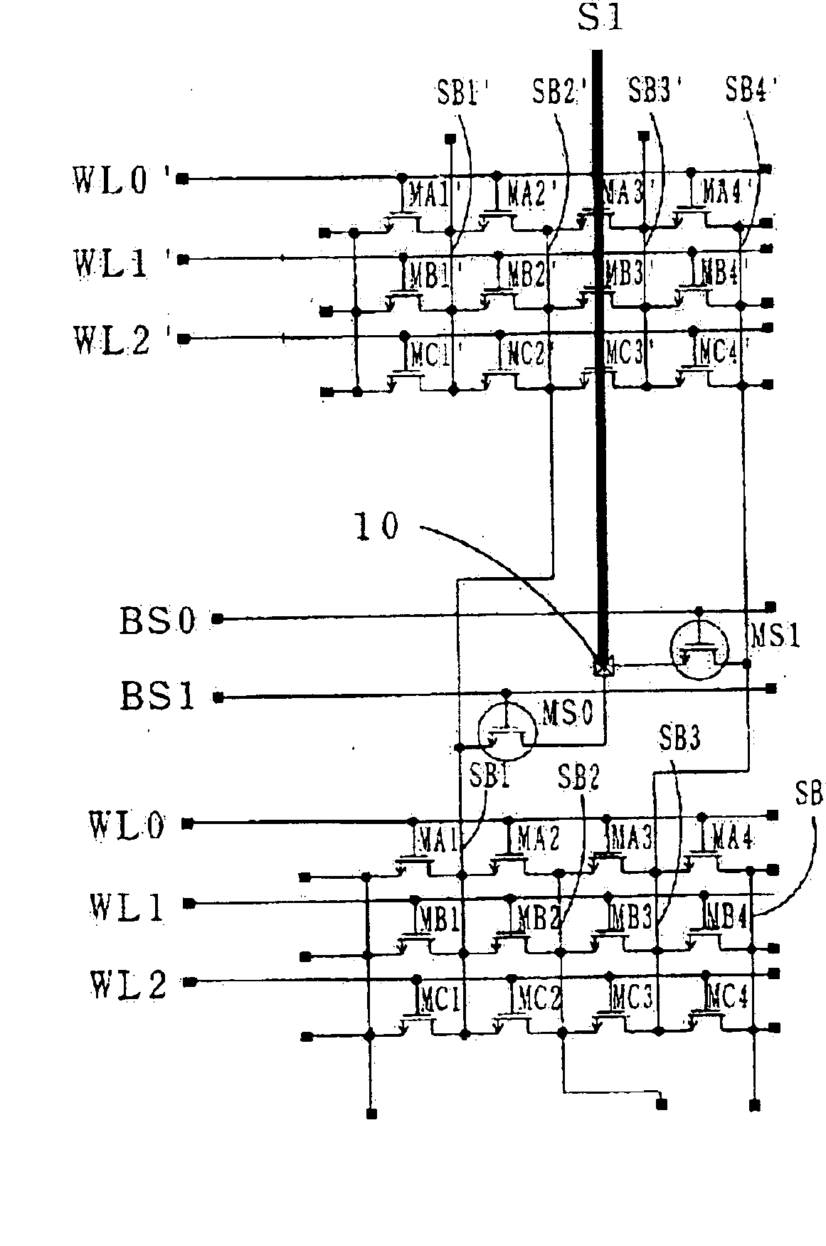
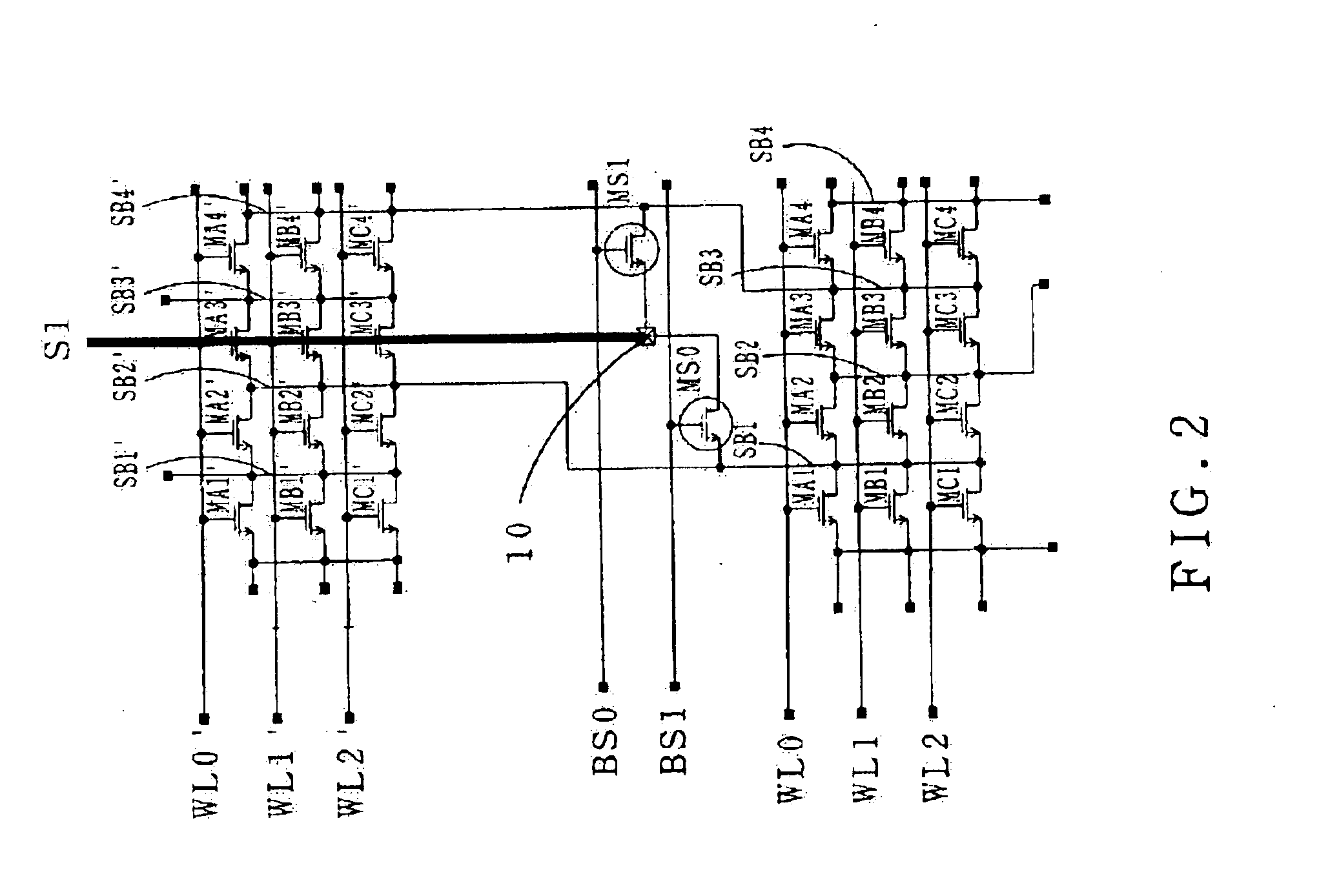
The bank array architecture of a memory cell array containing bank selection structure is disclosed in the present invention. The first embodiment shown in FIG. 2, a first plurality of memory cells MA1, MA2, MA3, MA4, are connected in parallel to a second plurality of memory cells MB1, MB2, MB3, MB4, and a third plurality of memory cells MC1, MC2, MC3, MC4. Each memory cell of the first, second and third plurality of memory cells is coupled to two adjacent lines constituting a memory bank (herein named first memory bank). A memory array consisting of a plurality of memory banks. Furthermore, with their individual gate terminals, the memory cells MA1 to MA4 are commonly connected to corresponding word line WL0. Similarly, the gate terminals of the memory cells MB1 to MB4 are commonly connected to corresponding word line WL1, and those of the memory cells MC1 to MC4 are commonly connected to corresponding word line WL2.

On the other hand, an adjacent memory bank (herein named second me...

second embodiment

The second embodiment shown in FIG. 4 illustrates the amount reduction of the contact number and pitch release of metal contact in the present invention. In the second embodiment, the metal bit line S1 is coupled to two inter-bank selection transistors MS0 and MS5, and four intra-bank selection transistors MS1, MS2, MS3, and MS4 through a contact 20. Similar to FIG. 2, the gate terminal of inter-bank selection transistor MS0 is connected to bank selection line BS0. The individual gate terminals of intra-bank selection transistors MS1 and MS2 are commonly connected to bank selection line BS1. The individual gate terminals of intra-bank selection transistors MS3 and MS4 are commonly connected to bank selection line BS2. The gate terminal of inter-bank selection transistor MS5 is connected to bank selection line BS3. The metal bit line S1 is connected to second or first terminals of the intra-bank and inter-bank selection transistors MS0 to MS5. In the embodiment, the individual first ...


PUM


Abstract

The present invention provides a read-only memory array having a flat-type structure. The read-only memory array comprises at least two memory banks having a plurality of memory cells. At least two inter-bank transistors are coupled to the two memory banks and shared by the two memory banks. Each inter-bank transistor is used for enabling to select the memory cells of the two memory banks. At least a contact commonly is coupled to the two memory banks through the two inter-bank transistors.

Description

BACKGROUND OF THE INVENTION1. Field of the InventionThe invention relates to mask read-only memory, and more particularly to mask read-only memory having flat-type bank select.2. Description of the Prior ArtThere are several read-only memory (ROM) cell structures are well known in application. One approach is referred to as the flat-type ROM design. With the requirement of better memory cell efficiency, the cell pitch and bank height become the key factor to be considered. While the memory cell is shrinking down, the contact size and metal pitch become the limit of it. On the other hand, memory array used to use LOCOS-type MOS for the bank selection transistors, which causes difficulties in the reduction of the layout area.Memory devices with flat-type ROM design are well documented. For example, a prior technique is illustrated in U.S. Pat. No. 5,117,389 of Yiu, entitled “Flat-Cell Read-Only-Memory Integrated Circuit”. Shown in FIG. 1, the number of bank selection transistors utili...

Claims


Application Information

Patent Timeline
IPC IPC(8): G11C8/00G11C8/12G11C17/14G11C17/12G11C17/08G11C17/18
CPCG11C8/12G11C17/18G11C17/12
Inventor CHEN, JING-WENNI, FUL-LONGYANG, NIEN-CHAO
Owner MACRONIX INT CO LTD
Why Eureka
Try Eureka