
Method of deducing equivalent circuit and system for the same

a technology of equivalent circuits and equivalent circuits, applied in the direction of testing circuits, resistance/reactance/impedence, instruments, etc., can solve the problems of increasing product development costs, reducing competitive power against products of other companies, and lsi giving radiation and conduction noises to other electronic equipment. achieve the effect of ensuring the intended accuracy

Inactive Publication Date: 2005-03-22
HITACHI LTD
View PDF7 Cites 15 Cited by
  • Summary
  • Abstract
  • Description
  • Claims
  • Application Information

AI Technical Summary

Benefits of technology

A first object of the present invention is to provide a method of calculating an equivalent circuit that reduces the number of elements constituting a network to a large extent, while securing an intended accuracy.

Problems solved by technology

Accompanied with the tendency to a higher speed in the LSI operational frequency, there emerges a problem of (EMI) Electro Magnetic Interference, that electronic equipment incorporating such a high speed LSI gives radiation and conduction noises to the other electronic equipment.
However, such a symptomatic measure invites an increase of product development cost and an extension of development term, which leads to lowering a competitive power against products of other companies.
In consequence, the circuit analysis using the conventional technique requires much more memory capacity and analyzing time.
If the memory capacity and analyzing time are restricted to a practically available size and period, a complicated modeling with a great number of elements will become impossible.
Accordingly, the modeling will have to be a simplified one; the accuracy of analysis will become inferior.

Method used


Image

  • Method of deducing equivalent circuit and system for the same
  • Method of deducing equivalent circuit and system for the same
  • Method of deducing equivalent circuit and system for the same

Examples


second embodiment

Next, the second embodiment relating to the invention will be described. In this embodiment is shown a case that executes the circuit analysis by using the equivalent circuit attained according to the foregoing method.

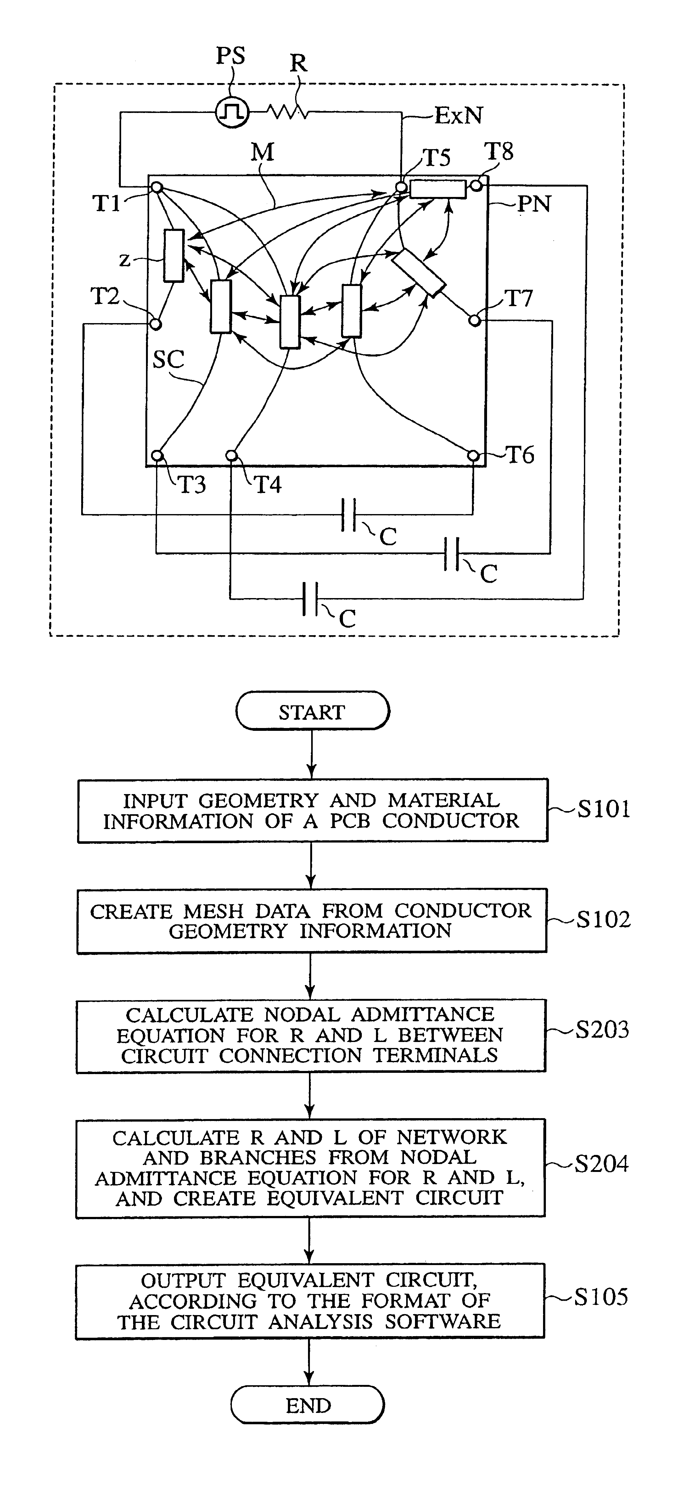
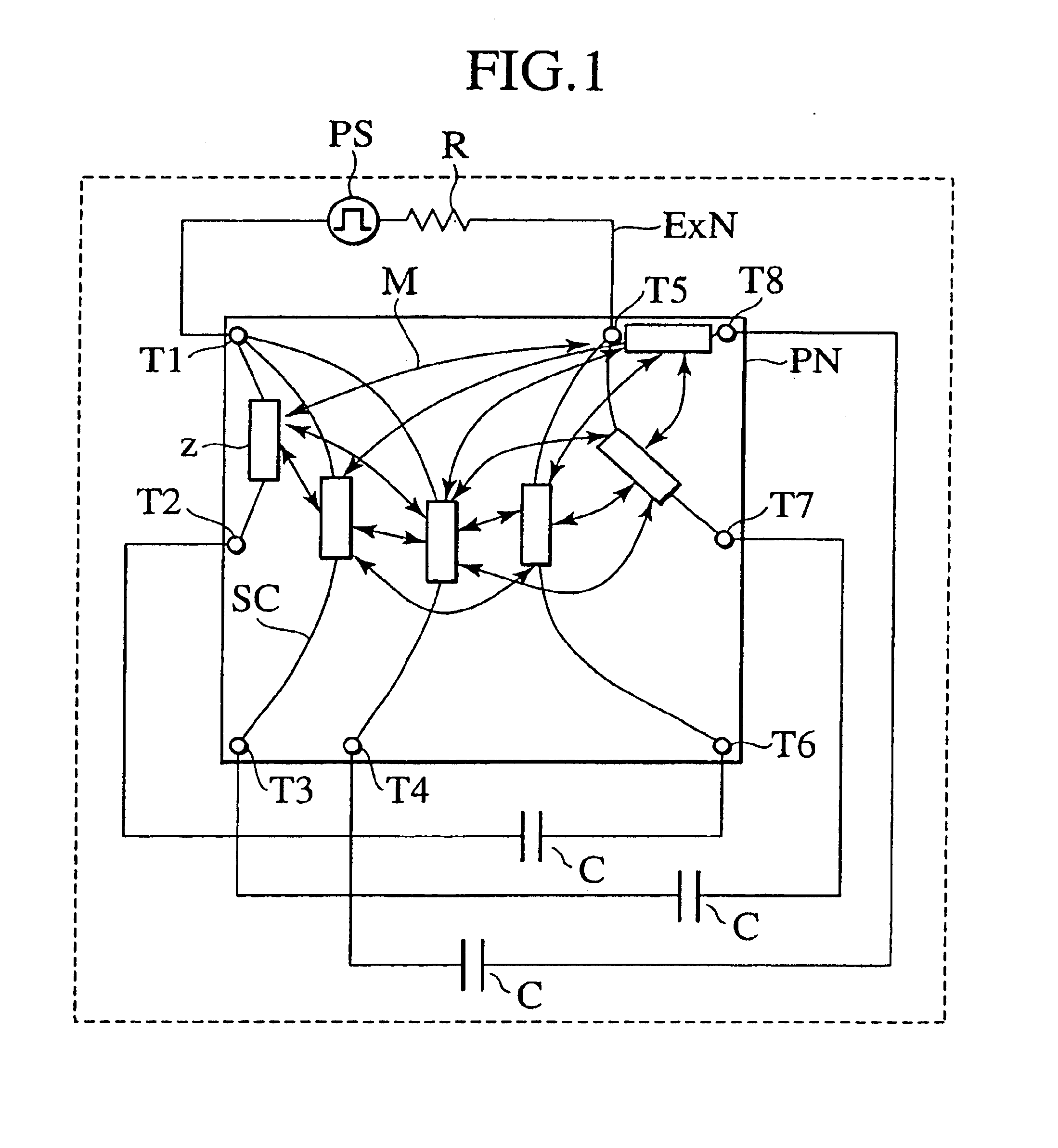
FIG. 17 illustrates a network image by the circuit analysis that used the equivalent circuit to the PCB in FIG. 3B. As shown in FIG. 17, a square-wave voltage source PS and a resistor R are connected in series between the terminals T1 and T5. Capacitors C of the same capacitance 0.1 nF are each connected between the terminals T2 and T6, between T3 and T7, and between T4 and T8 . The resistor R has a resistance, for example, 5Ω. FIG. 18 illustrates a voltage waveform of the voltage source PS in the circuit analysis that used the equivalent circuit according to this embodiment. FIG. 19 illustrates a current waveform that flows through the voltage source PS. From the current waveform in FIG. 19, even a simple network composed of the voltage source, resistors, and capacito...


PUM


Abstract

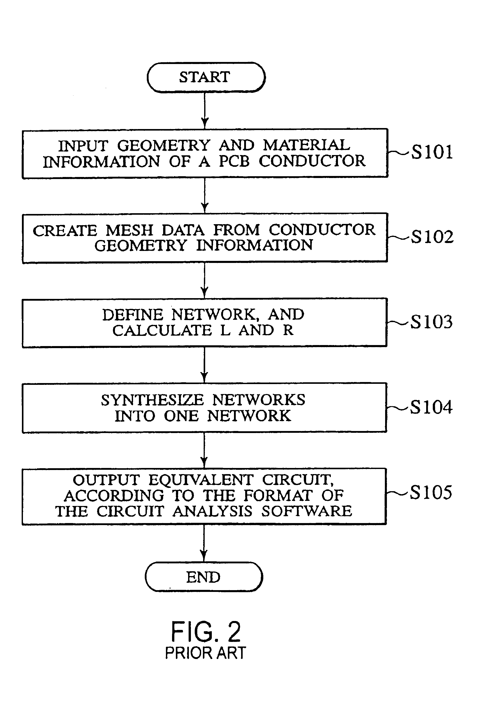
The invention provides a method of calculating an equivalent circuit, which reduces the number of elements constituting a network to a large extent with a target accuracy secured. The method of the invention calculates an equivalent circuit by a computer, with regard to an object that has a conductor, a dielectric to support the conductor, and plural input / output terminals to the outside. Step 1 in the method receives inputs of geometry information to specify a shape of a conductor in a circuit board being the object of determining the equivalent circuit, and material information to specify a material of the circuit board; Step 2 partitions the shape of the objective conductor into meshes on the basis of the geometry information received, and creates mesh data to be expressed; Step 3 calculates a nodal admittance matrix from the mesh data, and stores the result; step 4 calculates the number of nodes and the number of independent networks on the basis of the mesh data, determines an incidence matrix, and determines the structure of an equivalent network by means of the calculated nodal admittance matrix and incidence matrix; and Step 5 determines the values of elements of the equivalent network.

Description

BACKGROUND OF THE INVENTIONThis invention relates to a technique that represents a network with an equivalent circuit, and more particularly to a technique that represents an equivalent circuit with few components with an accuracy secured.Accompanied with the tendency to a higher speed in the LSI operational frequency, there emerges a problem of (EMI) Electro Magnetic Interference, that electronic equipment incorporating such a high speed LSI gives radiation and conduction noises to the other electronic equipment. Efforts to solve this EMI problem have been made for a measure that suppresses radiation noises and / or reduces conduction noises, individually to prototypes and products by means of a trial-and-error method. However, such a symptomatic measure invites an increase of product development cost and an extension of development term, which leads to lowering a competitive power against products of other companies. Thus, there arises a necessity of a design system, whereby suppres...

Claims


Application Information

Patent Timeline
IPC IPC(8): G06F17/50
CPCG06F17/5036G06F30/367
Inventor MABUCHI, YUICHIFUKUMOTO, HIDESHI
Owner HITACHI LTD
Learn More