Apparatus for peeling protective sheet

a protective sheet and apparatus technology, applied in electrical apparatus, basic electric elements, semiconductor devices, etc., can solve problems such as chip breakage and damage, troublesome transmission and wafer breakage, etc., and avoid breakage and damage of ultra thin chips

Inactive Publication Date: 2005-03-29
LINTEC CORP
View PDF6 Cites 5 Cited by
  • Summary
  • Abstract
  • Description
  • Claims
  • Application Information

AI Technical Summary

Benefits of technology

The present invention was devised in view of the above problems. An object of the present invention is to provide a method and an apparatus for peeling a protective shee

Problems solved by technology

With this type of method, however, there is a concern that transfer trouble and wafer breakage, etc. will occur when using an ultra-thin wafer as a result of the warping of the wafer.
When performing this type of peeling, however, if the adhesive tape is pulle

Method used


Image

  • Apparatus for peeling protective sheet
  • Apparatus for peeling protective sheet
  • Apparatus for peeling protective sheet

Examples


Embodiment Construction

Hereinafter, one embodiment of the present invention will be described with reference to accompanying drawings.

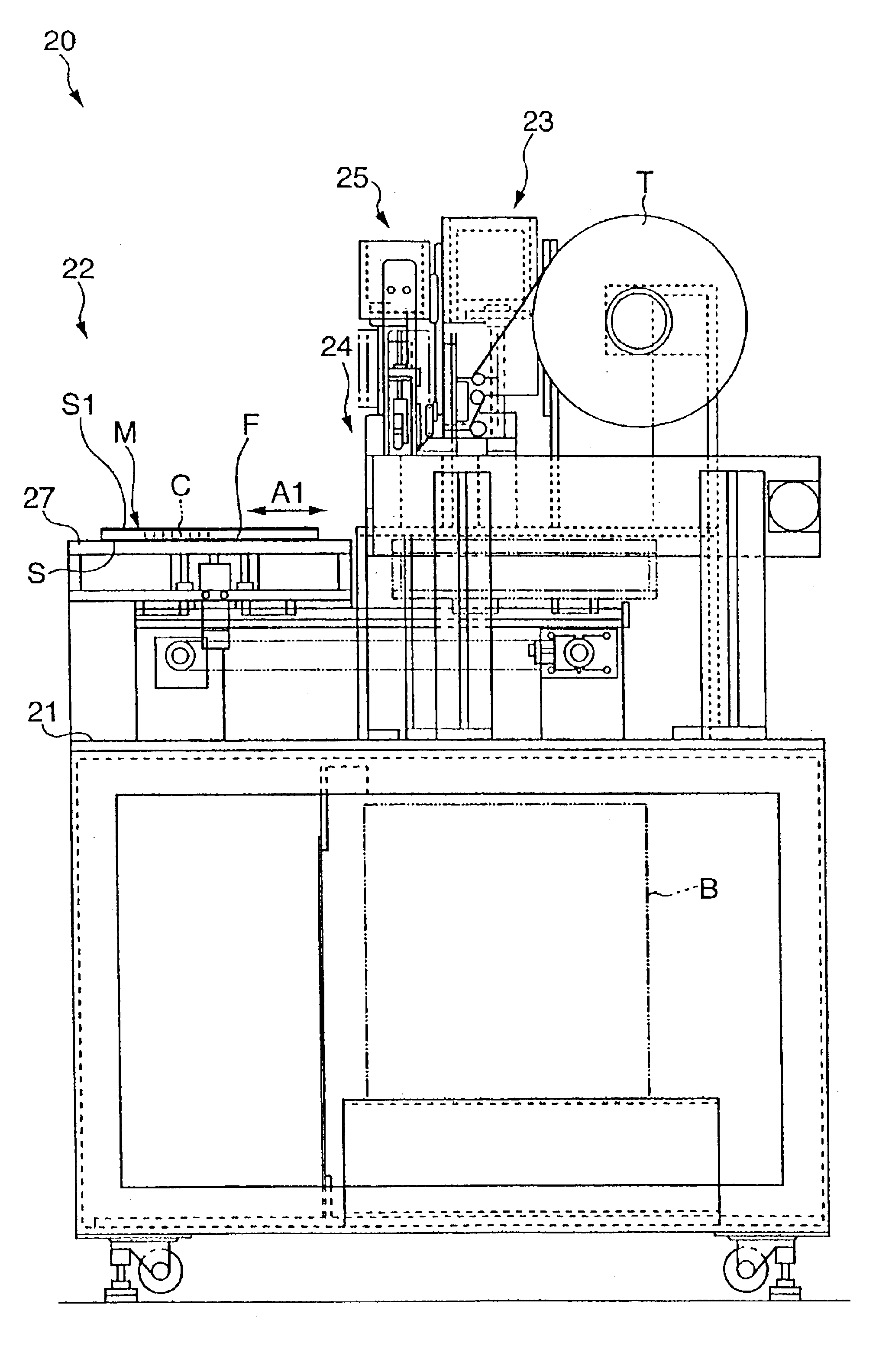
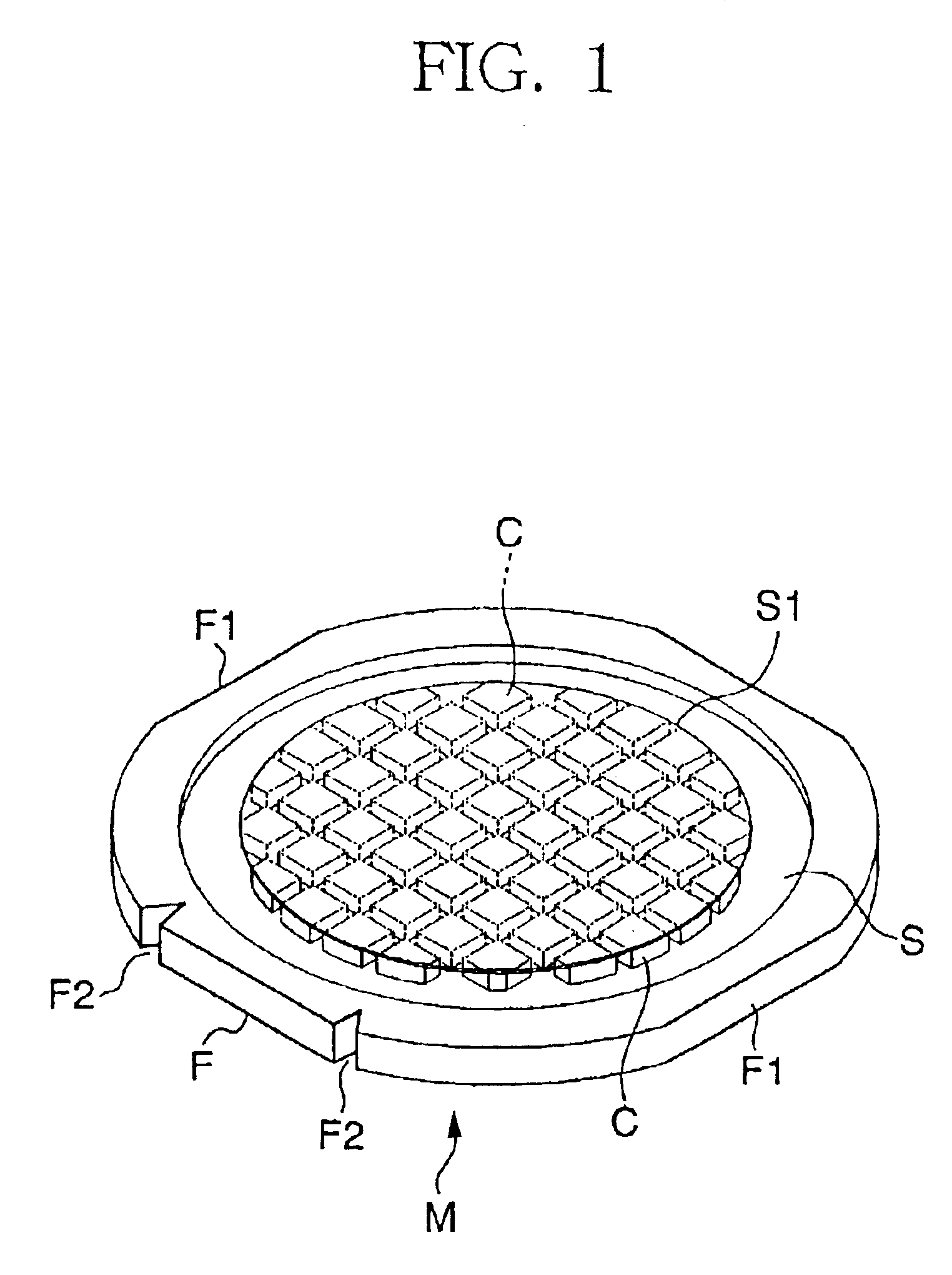
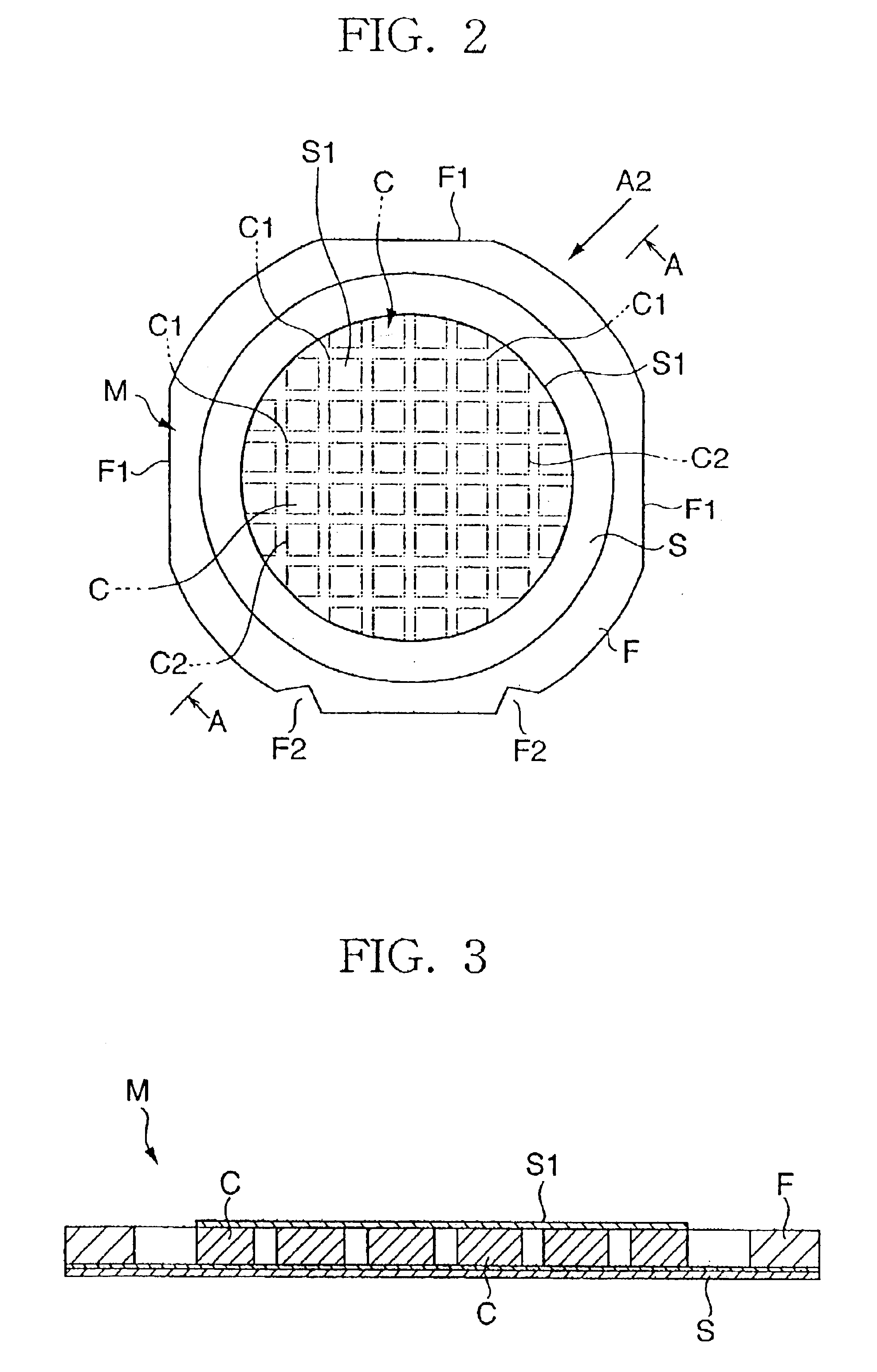
FIG. 1 shows a schematic perspective view of an attachment body M formed by attaching chips, to which a method according to the present invention is applied, to a ring frame using an adhesive sheet. A dicing before grinding method has been conducted on the chips, and a protective sheet has been attached on surfaces of the chips formed circuit patterns. FIGS. 2 and 3 show its top view and sectional view. In these figures, a plurality of chips C to which the dicing before grinding method has been conducted is attached using an adhesive sheet S which is provided on the lower surface side of a ring frame F. A circuit pattern is formed on the surface (the upper surface in FIG. 1) of the chips C, for which ultra thin chips with a thickness of 30 μm to 150 μm are applicable, and a protective sheet S1 is attached.

The protective sheet S1, which is attached to the chips C, is peeled ...


PUM

PropertyMeasurementUnit
Electric potential / voltageaaaaaaaaaa
Lengthaaaaaaaaaa
Crystal orientationaaaaaaaaaa

Abstract

Chips C which have already been diced are attached to a ring frame F using an adhesive sheet, and a protective sheet S1 is attached to a circuit pattern surface of the chips C. The chips C, along with a ring frame F, are held in place on a table 27 of a protective sheet peeling apparatus 20. A supply portion for an adhesive tape T is disposed in the vicinity of a table 24, and the supplied adhesive tape T is attached to the protective sheet S1. When the protective sheet S1 is peeled from the circuit pattern surface, peeling starts from corner portions of the chips C or opposing corner positions by pulling the adhesive tape T.

Description

BACKGROUND OF THE INVENTION1. Field of the InventionThe present invention relates to a method and an apparatus for peeling a protective sheet that is attached to the circuit pattern surfaces of chips after a dicing before grinding method has been conducted.2. Description of the Related ArtAs a method for producing a semiconductor wafer, a method has been known for forming a circuit pattern on the surface of a large diameter disc-shaped wafer, grinding the backside while the surface is protected by a protective tape, and peeling the protective sheet. After the semiconductor wafer is attached to a ring frame using an adhesive sheet, it is diced into a plurality of chips in cube-shape using a dicing cutter, and is transferred in this condition to the next processes of washing, drying, die bonding, etc.With this type of method, however, there is a concern that transfer trouble and wafer breakage, etc. will occur when using an ultra-thin wafer as a result of the warping of the wafer. Rec...

Claims


Application Information

Patent Timeline
IPC IPC(8): B29C63/00H01L21/00H01L21/68H01L21/67H01L21/301H01L21/304H01L21/78
CPCB29C63/0013H01L21/67132H01L21/6835H01L21/6836H01L21/304Y10T29/41H01L2221/68327H01L2221/6834H01L2221/6839Y10S438/977H01L21/78Y10T83/04
Inventor TSUJIMOTO, MASAKI
Owner LINTEC CORP
Why Eureka
Try Eureka