
Methods for providing an integrated circuit package with an alignment mechanism

a technology of alignment mechanism and integrated circuit, which is applied in the direction of printed circuit aspects, sustainable manufacturing/processing, final product manufacturing, etc., can solve the problems of lga package edges not always true, difficult to align with respect to the environment in which they operate, and base becoming out of squar

Inactive Publication Date: 2005-03-29
AVAGO TECH WIRELESS IP SINGAPORE PTE
View PDF4 Cites 9 Cited by
  • Summary
  • Abstract
  • Description
  • Claims
  • Application Information

AI Technical Summary

Benefits of technology

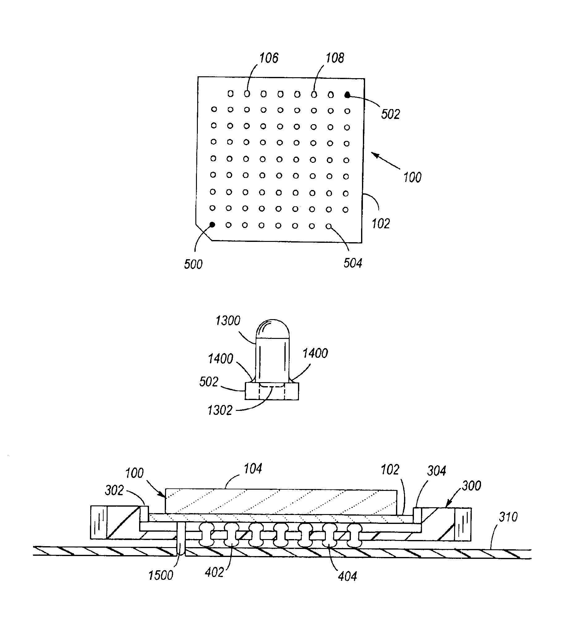
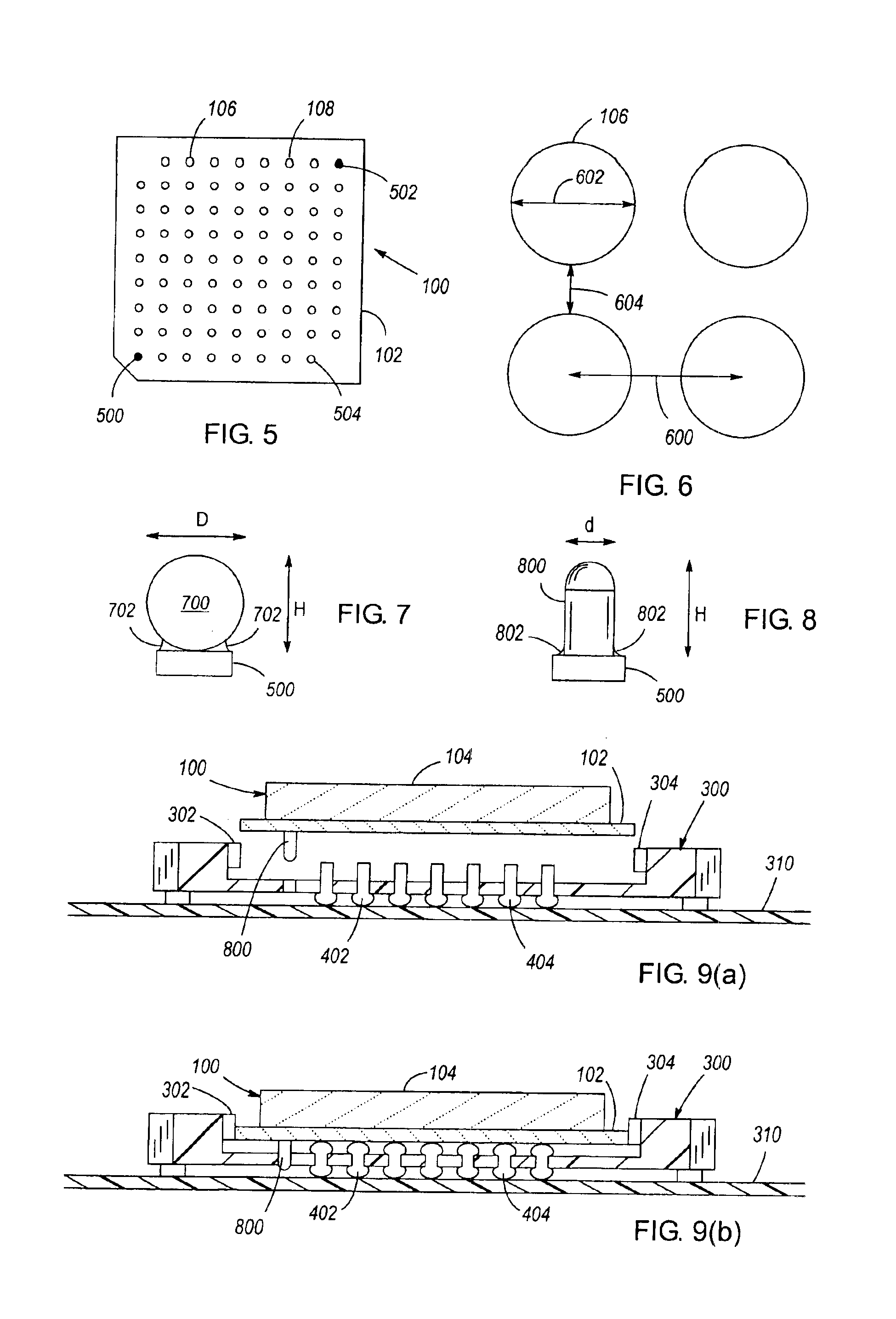
In one embodiment, a pattern of contact pads and number of annular ring shaped alignment pads are applied to a surface of an integrated circuit package, with the number of annular ring shaped alignment pads being applied to the surface at known locations with respect to the pattern of contact pads. The annular ring shaped alignment pads are provided as a means for attaching alignment members such as balls or bullets to the integrated circuit package. The annular ring shape of each alignment pad helps to center an alignment member which is attached to it, thereby providing a more precise relationship between the location of the alignment member and the package's pattern of contact pads.
In another embodiment, a number of alignment members are attached to an integrated circuit package after heating a wetting media (e.g., a paste solder) which is applied to a number of annular ring shaped alignment pads provided on the integrated circuit package. The number of annular ring shaped alignment pads are provided at known locations with respect to a pattern of contact pads which is also provided on the integrated circuit package. Use of the wetting media is advantageous in that 1) surface tension of the heated wetting media helps to center the alignment members over the alignment pads as 2) the wetting action of the wetting media seats the alignment members on the alignment pads. Precise alignment between the alignment members and the pattern of contact pads may therefore be maintained.

Problems solved by technology

One problem with LGA packages (including the subset of CLGA packages) is that they are difficult to align with respect to the environments in which they operate.
First, the edges of an LGA package are not always true, and do not always bear a precise relationship to the LGA package's contact pads.
During the firing process, the base is subject to shrinkage which can result in 1) the base becoming out of square, and 2) the base having skewed, curved or wavy edges.
Since no two bases shrink in precisely the same way, it is difficult to design a socket such that each and every LGA package will fit into it the same way.
A second problem which contributes to the misalignment of an LGA package within a socket is that the contact pads which are applied to LGA packages are becoming smaller, and are achieving a finer pitch.

Method used


Image

  • Methods for providing an integrated circuit package with an alignment mechanism
  • Methods for providing an integrated circuit package with an alignment mechanism
  • Methods for providing an integrated circuit package with an alignment mechanism

Examples


Embodiment Construction

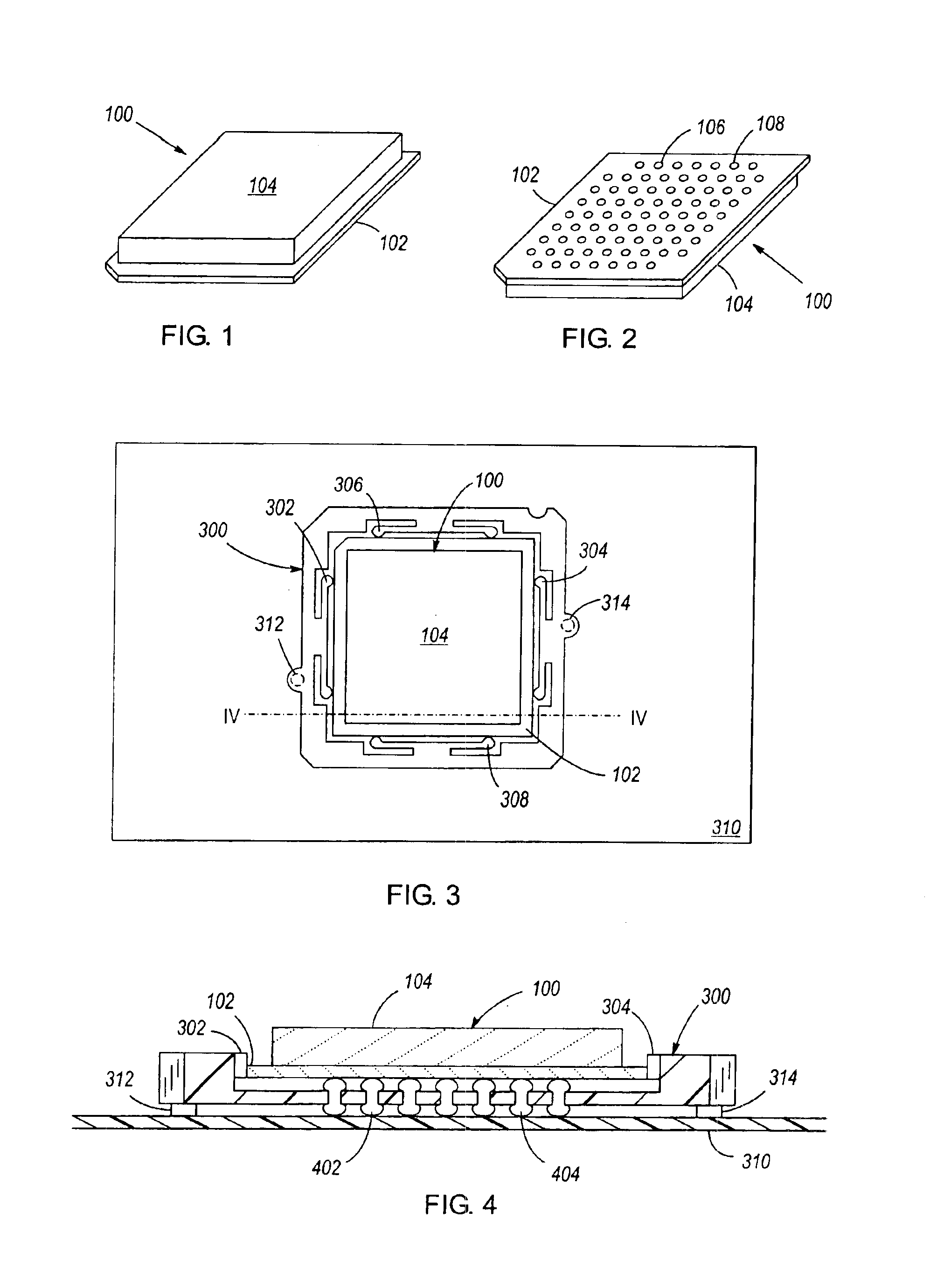
An integrated circuit package 100 is generally illustrated in FIGS. 1 & 2. By way of example, the package 100 is shown to be a ceramic land grid array (CLGA) package (although the alignment methods and apparatus disclosed herein may be used in conjunction with a variety of integrated circuit packages, such as other LGA packages, BGA packages, et cetera). The CLGA package 100 comprises a ceramic base 102 and a lid 104. An integrated circuit is mounted to the top surface of the ceramic base 102, beneath the lid 104. The integrated circuit is then connected to contacts which terminate in a contact pad pattern which is applied to (e.g., screened) onto the bottom surface of the ceramic base 102 (FIG. 2). Each contact pad 106, 108 may be formed of gold, or any other conductive material which will provide sufficient electrical contact between the integrated circuit and an adjacent electrical / mechanical interface to which it is connected.

In FIGS. 3 & 4, the CLGA package 100 of FIGS. 1 & 2 i...


PUM


Abstract

An integrated circuit package is provided with an alignment mechanism by 1) heating a wetting media that has been applied to a number of annular ring shaped alignment pads provided on the integrated circuit package, at known locations with respect to a pattern of contacts pads that is provided on the integrated circuit package, and then 2) while the wetting media is heated, attaching a number of alignment balls or alignment bullets to the annular ring shaped alignment pads.

Description

FIELD OF THE INVENTIONThe invention pertains to aligning an integrated circuit package with an interface. More particularly, the invention pertains to methods and apparatus which enable an integrated circuit package to be aligned with an interface when 1) the package's contacts do not provide a sufficient alignment means, and / or 2) the package's edges do not provide a sufficient alignment means (i.e., when the locations of the package's edges with respect to its contacts are not known).BACKGROUND OF THE INVENTIONThere are a number of ways to achieve better performance from an integrated circuit. One way is to reduce the impedance of wire routes, thus enabling circuit signals to propagate more quickly. The impedance of wire routes may be reduced, for example, by minimizing the impedance of wire routes may be reduced, for example, by minimizing the heights of contacts which couple an integrated circuit (IC) to its environment (e.g., by minimizing the heights of contacts provided on an...

Claims


Application Information

Patent Timeline
Patent Type & Authority Patents(United States)
IPC IPC(8): H01L21/60H01L21/02H01L23/485H01L23/48H01L21/48H05K3/30H05K3/34H05K3/32H01L23/12
CPCH01L21/4853H01L24/11H05K3/303H01L24/02H01L2924/01033H01L2224/0401H01L2224/13099H01L2924/01004H01L2924/01005H01L2924/01006H01L2924/01028H01L2924/01029H01L2924/01047H01L2924/01078H01L2924/01079H01L2924/014H01L2924/14H01L2924/3011H05K3/325H05K3/3436H05K2201/0969H05K2201/09781H05K2201/10234H05K2201/10325H05K2203/048H05K2203/167Y02P70/50
Inventor D'AMATO, GERALD J.CHRISTENSEN, SARI K.BUTEL, NICOLE
Owner AVAGO TECH WIRELESS IP SINGAPORE PTE
Learn More