
Substrate dual-side processing apparatus

a processing apparatus and substrate technology, applied in the direction of instruments, load-engaging elements, cleaning using liquids, etc., can solve the problems of low throughput, complex and large, etc., and achieve the effect of high throughput and accurate substrate revering operation

Inactive Publication Date: 2005-04-05
TOKYO ELECTRON LTD
View PDF21 Cites 81 Cited by
  • Summary
  • Abstract
  • Description
  • Claims
  • Application Information

AI Technical Summary

Benefits of technology

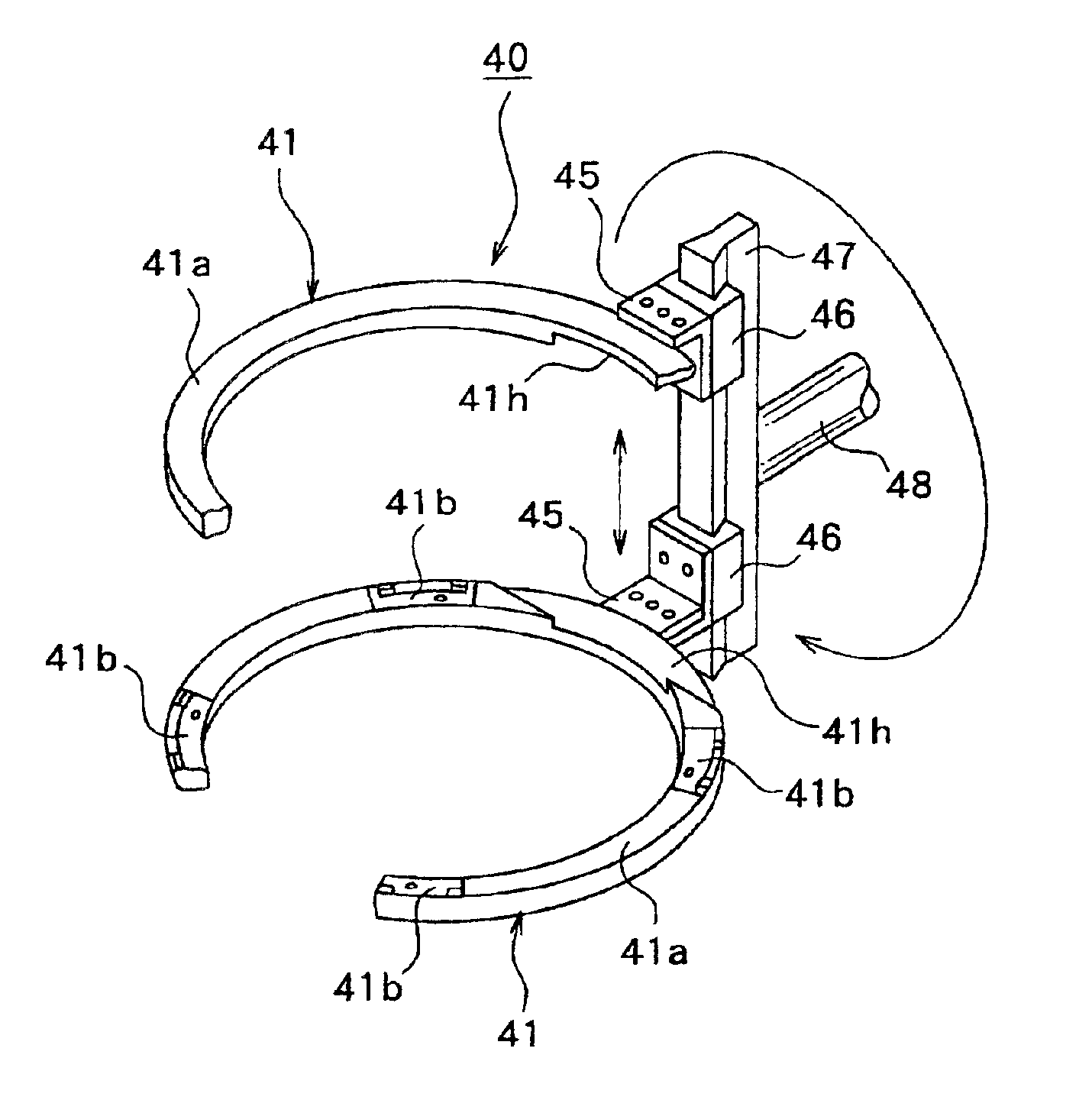
The present invention provides an apparatus for processing substrates on both sides with a compact structure and less driving mechanisms for accurate substrate revering operation, aiming at high throughput. The apparatus includes a processor for applying a specific process to the front and rear surfaces of a substrate, a reversing unit for reversing the substrate, and a substrate-transfer mechanism for transferring the substrate between the processor and the reversing unit. The reversing unit has a holder for holding the substrate and a rotating mechanism for rotating the substrate while held by the holder. This allows for efficient and accurate substrate reversing and transferring between the processor and the reversing unit.

Problems solved by technology

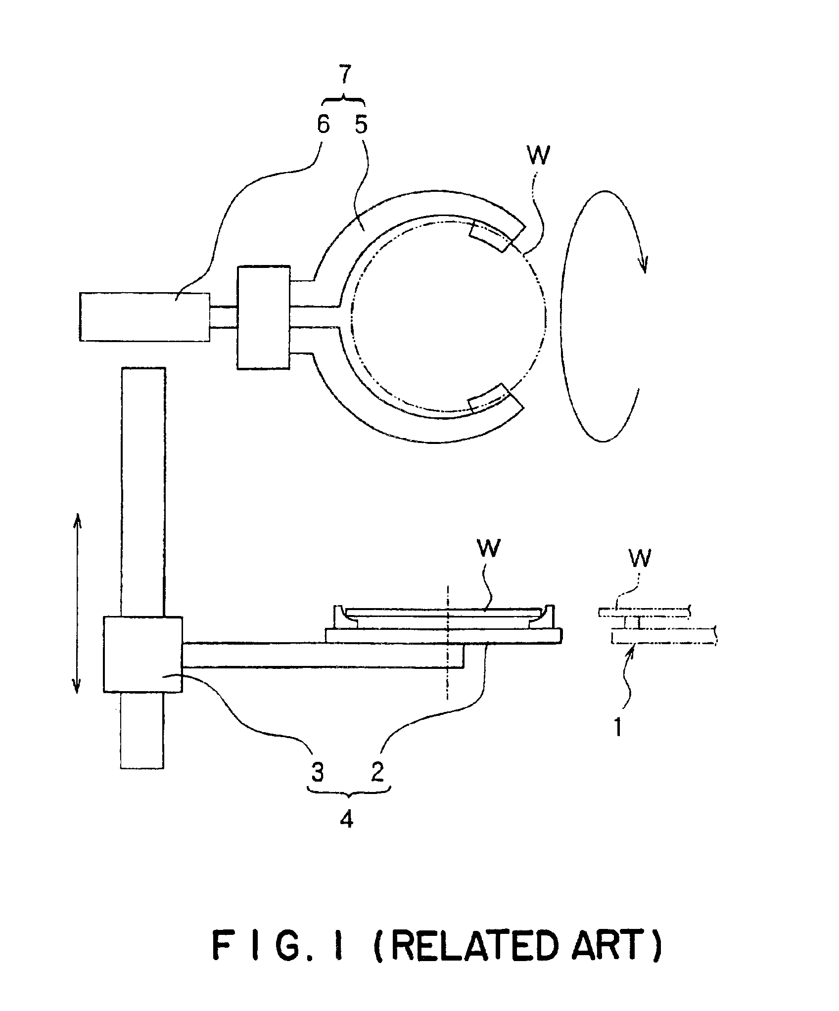
1 is, however, complex and large due to the existence of the substrate receiving / transferring mechanism 4 and the substrate reversing mechanism 7.
Moreover, both mechanisms 4 and 7 operate separately, so that it takes time for a reversing operation, thus causing a low throughput.
For example, the wafer W could be dropped if not accurately gripped by the reversing arm 5, thus being damaged.

Method used


Image

  • Substrate dual-side processing apparatus
  • Substrate dual-side processing apparatus
  • Substrate dual-side processing apparatus

Examples


Embodiment Construction

Preferred embodiments according to the present invention will be disclosed with reference to the attached drawings.

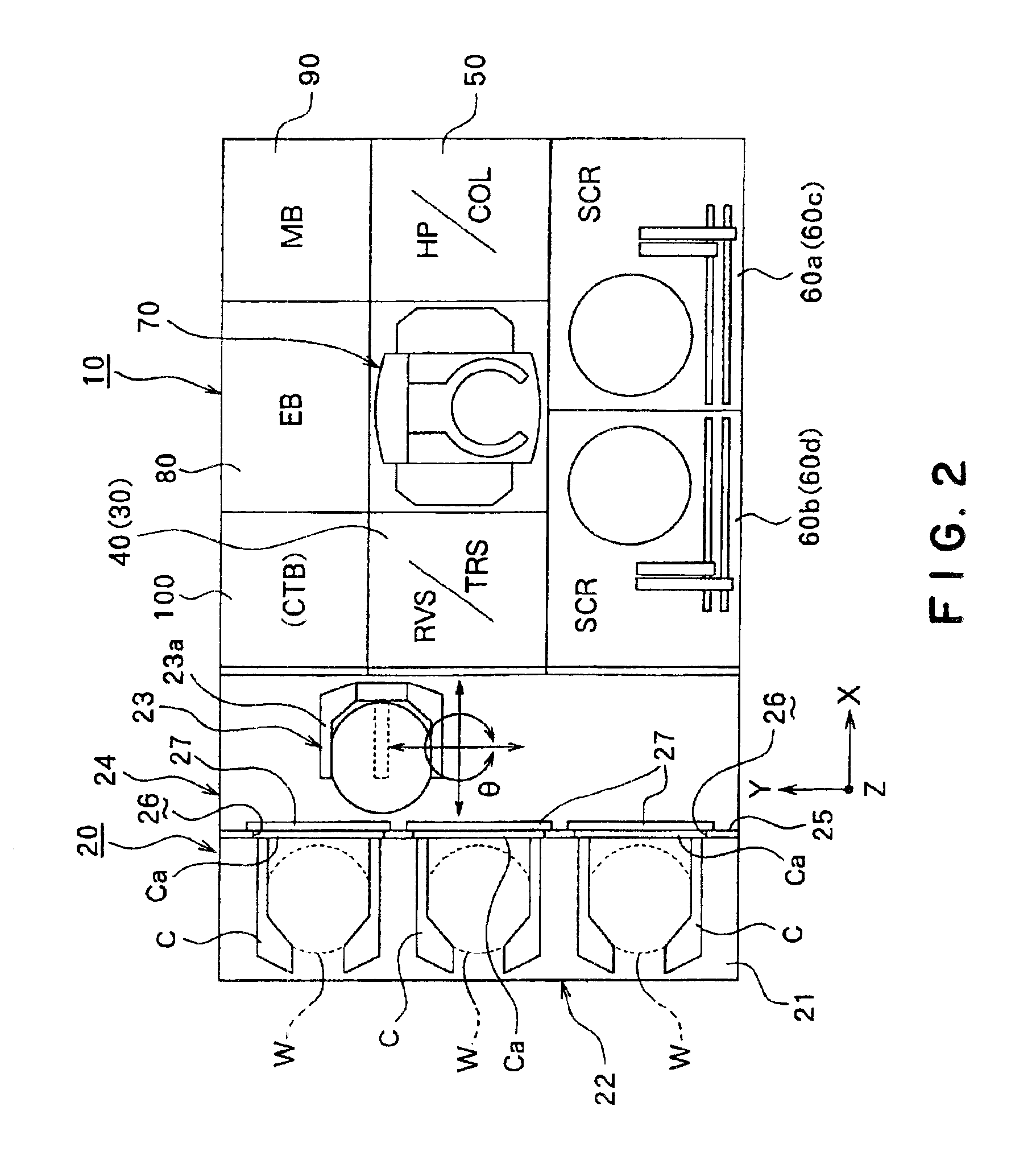
Disclosed below is an application of an apparatus for processing substrates on both sides to a cleaning system for sequential wafer transfer-in, cleaning, drying and transfer-out process.

The apparatus for processing substrates on both sides according to the present invention is termed a substrate dual-side processing apparatus hereinafter.

As shown in FIGS. 2 to 5, the cleaning system mainly consists of a cleaning section 10 for cleaning semiconductor wafers W as substrates to be processed and a transfer section 20 for transferring and receiving the wafers W to and from the cleaning section 10.

The transfer section 20 is equipped with a transfer unit 22 having a table 21 on which carriers C are arranged, a wafer transfer mechanism 23 for transferring the wafers W between the carries C and the cleaning section 10, and an interface unit 24 having a wafer transfer passage (n...


PUM


Abstract

A substrate dual-side processing apparatus has a processor to apply a specific process to a front surface and a rear surface of a substrate, a reversing unit to reverse the substrate and a substrate-transfer mechanism to transfer the substrate between the processor and the reversing unit. The reversing unit has a holder for holding the substrate when the substrate is being transferred to and from the substrate-transfer mechanism and a rotating mechanism for rotating the substrate, thus the substrate being reversed while held by the holders. The reversing unit may have a pair of holders for holding the substrate at the front and rear surfaces, a drive mechanism for driving the pair of holders so that the holders become close to or apart from each other and a rotating mechanism for rotating the substrate, thus the substrate being reversed while held by the holders.

Description

BACKGROUND OF THE INVENTIONThe present invention relates to an apparatus for processing substrates on both sides, or a substrate dual-side processing apparatus. Particularly, this invention relates to an apparatus for applying a specific process such as a cleaning process to substrates such as semiconductor wafers and LCD substrates on both sides.A specific procedure such as a cleaning process is applied to semiconductor wafers, LCD substrates, etc., in semiconductor device fabrication. Particularly, the cleaning process is applied to wafers on both sides before and after several types of fabrication processes, for high cleanliness on the front surface of each wafer on which semiconductor devices will be formed.A known substrate dual-side processing apparatus is a cleaning system equipped with a processor having several processing units for applying specific processes to wafers on both sides, a substrate transfer mechanism for transferring wafers to several processing units and a re...

Claims


Application Information

Patent Timeline
Patent Type & Authority Patents(United States)
IPC IPC(8): B08B3/02B08B1/04B08B11/00B08B11/02H01L21/687H01L21/67H01L21/677H01L21/304
CPCB08B1/04B08B3/02B08B11/02H01L21/68707Y10S134/902G02F2001/1316B08B2203/0288G02F1/1316B08B1/32H01L21/304
Inventor ISHIHARA, AKIRAMATSUSHITA, MICHIAKISAKATA, YUKIHIKO
Owner TOKYO ELECTRON LTD
Learn More