Post thermal treatment methods of forming high dielectric layers in integrated circuit devices

a technology of integrated circuit devices and dielectric layers, which is applied in the direction of electrical apparatus, nanotechnology, semiconductor devices, etc., can solve the problems of limited ability to scale silicon oxide layers to different sized semiconductor devices, large leakage current of silicon oxide, and the use of high dielectric layers as gate insulating layers,

Inactive Publication Date: 2005-04-05
SAMSUNG ELECTRONICS CO LTD
View PDF5 Cites 32 Cited by
  • Summary
  • Abstract
  • Description
  • Claims
  • Application Information

AI Technical Summary

Benefits of technology

The present invention relates to methods for forming high dielectric layers in integrated circuit devices and treating the high dielectric layers. In particular, various embodiments of the present invention relate to methods for treating high dielectric layers of integrated circuit devices, wherein the high dielectric layers may include aluminum oxide layers, yttrium oxide layers, hafnium oxide layers, and / or zirconium oxide layers. The embodiments of the present invention provide methods for nitriding, oxidizing, and / or annealing the high dielectric layers.
The various embodiments of the present invention involve methods for treating one or more high dielectric layers of one or more integrated circuit devices. The high dielectric layers may include layers of hafnium oxide, zirconium oxide, and / or Group 3 metal oxide layers, such as aluminum oxide and yttrium oxide. For the purposes of explaining the various embodiments of the present invention, the recitations of “Group 3 metal” means and includes all metals in Group 3 of the periodic table. This includes, for example, Sc, Y, La, Ac, B, Al, Ga, In, and Tl. For instance, in various embodiments of the present invention a high dielectric layer may include a nano laminate that includes a hafnium oxide layer or a zirconium oxide layer and a Group 3 metal oxide layer.
In various embodiments of the present invention, a method for treating one or more high dielectric layers of one or more integrated circuit devices involves the nitriding of a silicon substrate upon which the high dielectric layer is formed. The nitriding of the substrate may be performed, for example, by using a nitrogen plasma treatment, a thermal treatment in a nitrogen atmosphere, or a thermal treatment of a nitrogen layer formed on the substrate. Following nitriding, the silicon substrate and high dielectric layer are post treated by oxidizing the substrate to which the nitriding was applied, annealing the substrate to which the nitriding was applied, or by both oxidizing and annealing the substrate to which the nitriding was applied.
In certain embodiments of the present invention, the post treatment of a silicon substrate and high dielectric layer involves the annealing of the nitrided silicon substrate and high dielectric layer. The post treatment anneal may be performed in an atmosphere of inert gas or gases, heavy hydrogen, hydrogen, mixtures of nitrogen and hydrogen gas, or in a vacuum. The post treatment anneal following nitriding may be performed at temperatures at or between about 750° C. and about 1100° C.
In other embodiments of the present invention, the post treatment of a nitrided silicon substrate and high dielectric layer involves oxidizing the silicon substrate and high dielectric layer to which the nitriding was applied. The post treatment oxidizing may be performed using wet or dry oxidizing techniques to oxidize the silicon substrate where the high dielectric layer is formed. Oxidization of the silicone substrate and high dielectric layer may be performed with ozone, radical oxygen, and / or oxygen plasma. The oxidizing may be performed at or between temperatures of about 700° C. to about 900° C. in some embodiments.
Other embodiments of the present invention involve the post treatment oxidization of the silicon substrate and high dielectric layer to which nitriding was applied, followed by the annealing of the nitrided and oxidized silicon substrate and high dielectric layer. The oxidization may be performed using ozone, radical oxygen, and / or oxygen plasma, and may be carried out at or between temperatures of about 700° C. to about 900° C. The annealing process may be performed at or between temperatures of about 950° C. to about 1100° C.

Problems solved by technology

However, the dielectric constant of silicon oxide layers is about 3.9, which may pose some limitations on the ability to scale silicon oxide layers to different sized semiconductor devices.
In particular, the leakage current of silicon oxide can greatly increase as the thickness of the silicon oxide layer decreases.
The use of high dielectric layers as gate insulating layers, however, may have some problems.
For instance, if a BST layer, a TiO2 layer, or a Ta2O5 layer is directly deposited on a silicon substrate, interfacial characteristics with the silicon substrate may become poor and the leakage current may increase.
In addition, interface trap charge densities may increase and the mobility may decrease.
The use of aluminum oxide (Al2O3) as a high dielectric layer may provide a high thermal stability, however, aluminum oxide has a relatively low dielectric constant of about 11 and a threshold voltage that can be difficult to control.
However, zirconium oxide layers can react with polysilicon, therefore it may not be desirable to use zirconium oxide layers alone.
Hafnium oxide layers can become thick and can be easily crystallized, resulting in increases in the leakage current through grain boundaries.
In addition, the threshold voltages of devices including zirconium oxide layers and hafnium oxide layers can be difficult to control, making these compounds undesirable as high dielectric layers.

Method used


Image

  • Post thermal treatment methods of forming high dielectric layers in integrated circuit devices
  • Post thermal treatment methods of forming high dielectric layers in integrated circuit devices
  • Post thermal treatment methods of forming high dielectric layers in integrated circuit devices

Examples


Embodiment Construction

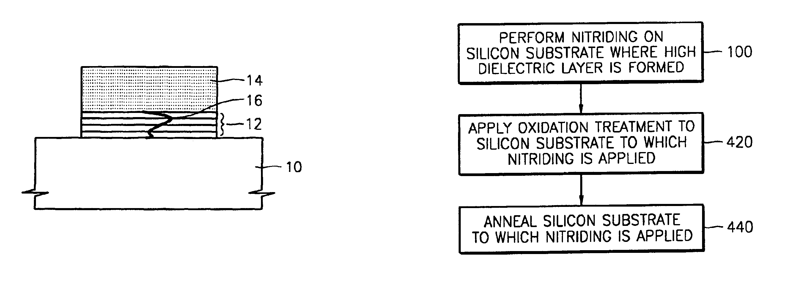
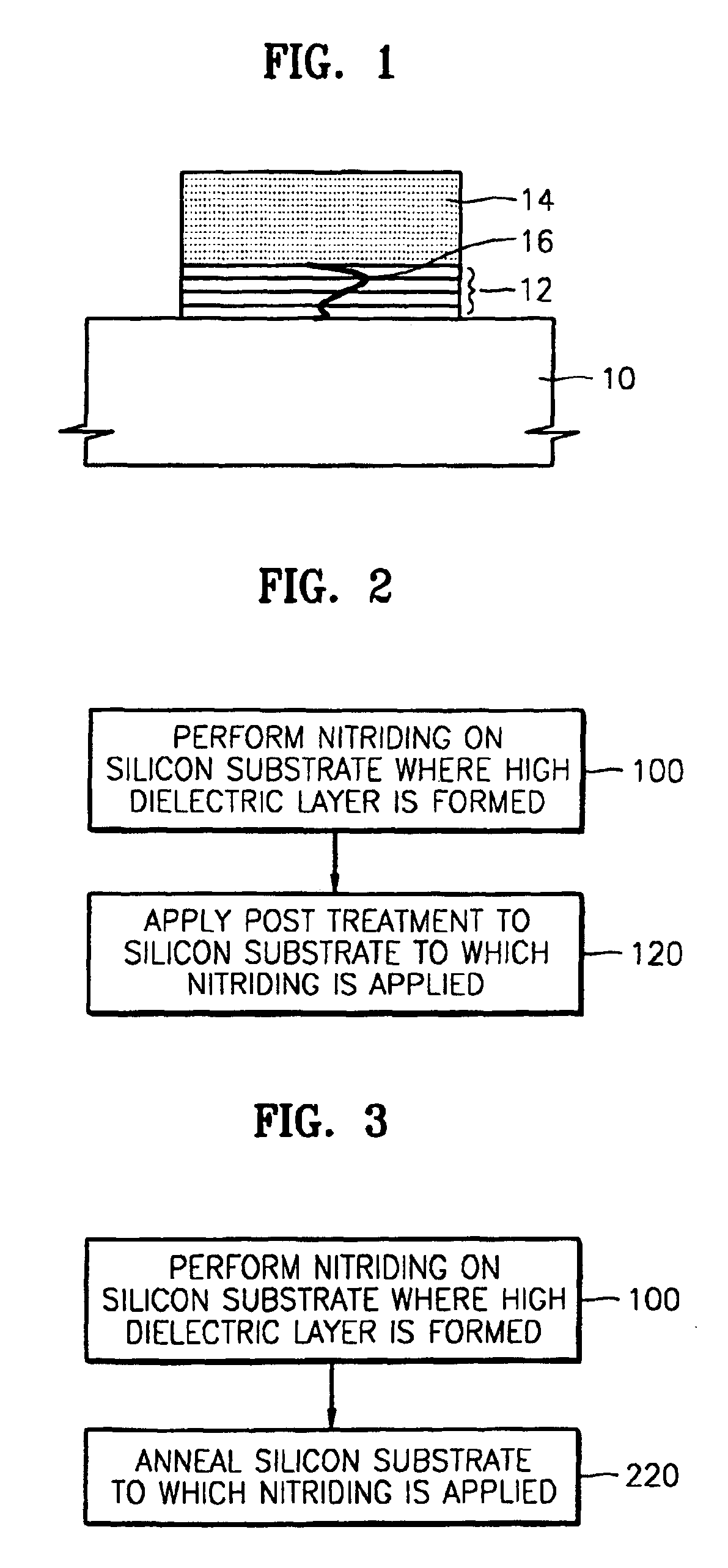
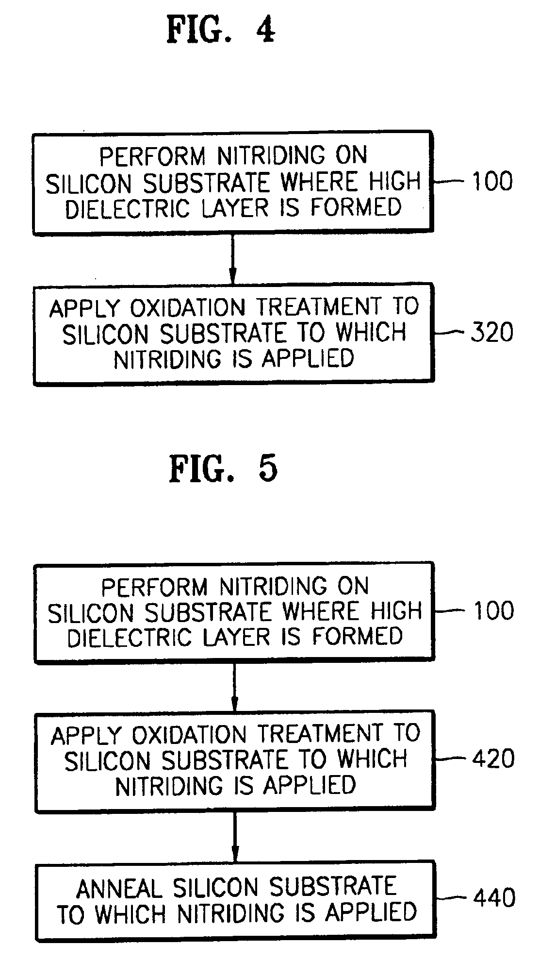
The present invention now will be described more fully hereinafter with reference to the accompanying drawings, in which embodiments of the invention are shown. This invention may, however, be embodied in many different forms and should not be construed as limited to the embodiments set forth herein; rather, these embodiments are provided so that this disclosure will be thorough and complete, and will fully convey the scope of the invention to those skilled in the art. In the drawings, the thickness of layers and regions are exaggerated for clarity. Like numbers refer to like elements throughout. It will be understood that when an element such as a layer, region or substrate is referred to as being “on” or “onto” another element, it can be directly on the other element or intervening elements may also be present. When an element such as a layer, region or substrate is referred to as being “directly on” another element, it is in direct contact with that other element.

FIG. 1 illustrat...


PUM

PropertyMeasurementUnit
temperatureaaaaaaaaaa

Abstract

High dielectric layers formed from layers of hafnium oxide, zirconium oxide, aluminum oxide, yttrium oxide, and/or other metal oxides and silicates disposed on silicon substrates may be nitrided and post thermally treated by oxidation, annealing, or a combination of oxidation and annealing to form high dielectric layers having superior mobility and interfacial characteristics.

Description

CROSS-REFERENCE TO RELATED APPLICATIONSThis application claims priority to Korean Patent Application No. 2002-54606, filed on Sep. 10, 2002 in the Korean Intellectual Property Office, the disclosure of which is incorporated herein in its entirety by reference.FIELD OF THE INVENTIONThe present invention relates to methods for forming dielectric layer structures in integrated circuit devices.BACKGROUND OF THE INVENTIONAs semiconductor devices become highly integrated and the thickness of gate insulating layers becomes smaller, new materials are being developed for the gate insulating layers. Silicon oxide (SiO2) layers may be used as gate insulating layers in today's semiconductor devices. Silicon oxides may be used as gate insulating layers because of their thermal stability, reliability, and ease of production. However, the dielectric constant of silicon oxide layers is about 3.9, which may pose some limitations on the ability to scale silicon oxide layers to different sized semicon...

Claims


Application Information

Patent Timeline
Patent Type & Authority Patents(United States)
IPC IPC(8): H01L21/28H01L21/02H01L29/51H01L21/314H01L21/316H01L29/40H01L21/318
CPCH01L21/28185H01L21/28202H01L21/3143H01L21/3144H01L21/31604H01L29/518H01L29/513H01L21/31645H01L21/3185H01L29/517H01L21/31641H01L21/02189H01L21/02192H01L21/02178H01L21/02181H01L21/022B82Y40/00H01L21/0234H01L21/02329H01L21/02337
Inventor JUNG, HYUNG-SUKLEE, NAE-INLEE, JONG-HOKIM, YUN-SEOK
Owner SAMSUNG ELECTRONICS CO LTD
Why Eureka
Try Eureka