Semiconductor device and design support method of electronic device using the same

Inactive Publication Date: 2005-04-05
HITACHI LTD
View PDF14 Cites 9 Cited by
  • Summary
  • Abstract
  • Description
  • Claims
  • Application Information

AI Technical Summary

Benefits of technology

[0018]Yet another embodiment of the present invention relates to a method for providing a component used in manufacturing an electronic device. The electronic device includes a semiconductor device and a printed circuit board. The method includes determining signal noise levels for each of a plurality of power terminals of the sem

Problems solved by technology

Although some terminals have a low power supply noise intensity and do not need any noise countermeasures, a bypass condenser or EMI filter is packaged for all the power supply and GND terminals since such terminals cannot be readily identified.
This increases the number of components used in assembling a module and the area of a substrate used for the module, which increases manufacturing costs and hinders the e

Method used


Image

  • Semiconductor device and design support method of electronic device using the same
  • Semiconductor device and design support method of electronic device using the same
  • Semiconductor device and design support method of electronic device using the same

Examples


embodiment 1

[0040

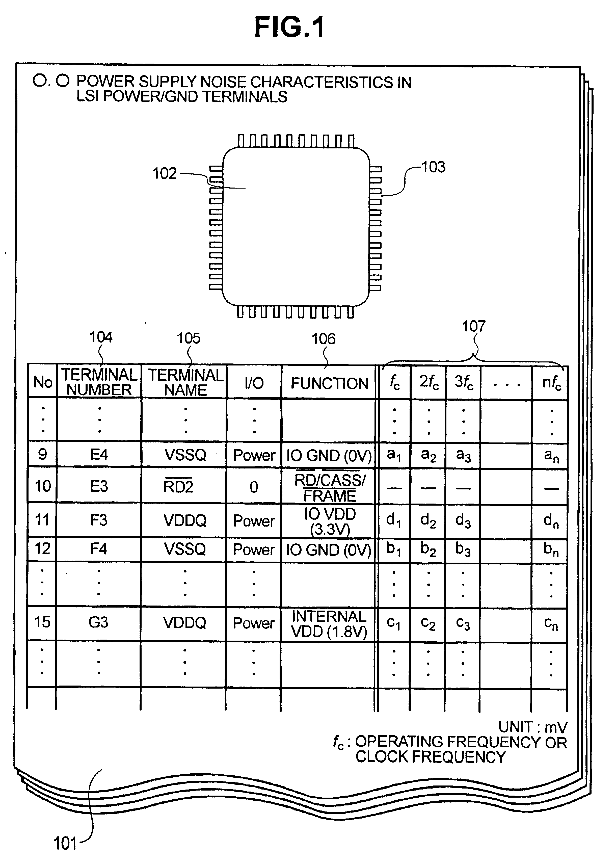
[0041]FIG. 1 depicts a diagram illustrating a data sheet, catalogue or specification providing information about electrical characteristics of predetermined power supply terminals of a semiconductor device.

[0042]A data sheet 101 shows the electric characteristics of all terminals in a semiconductor device, such as a microprocessor 102. The microprocessor has the characteristics described in the data sheet 101 and includes terminals 103. A column104 provides terminal numbers of the terminals 103 to identify the terminals. A column 105 provides terminal names of the corresponding terminals 103. A column 106 provides functions performed by the corresponding terminals 103. A column 107 provides a power supply noise intensity to an operating frequency in the corresponding terminals.

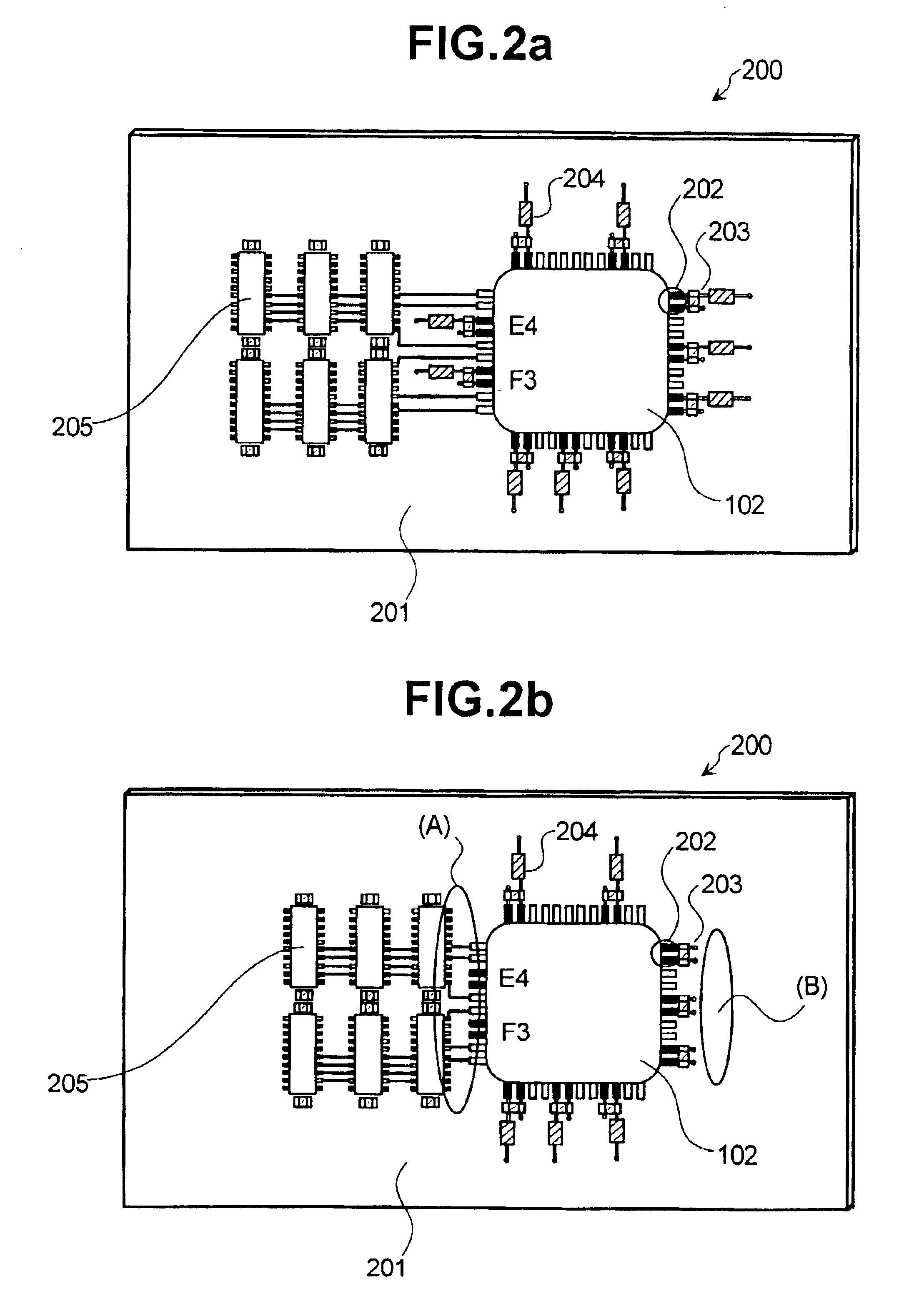
[0043]FIG. 2a depicts a device or module 200 including the microprocessor 102 and memories 205 packaged on a substrate or circuit board 201. Conventional data sheets of FIGS. 14 to 16 describe the module ...

embodiment 2

[0058

[0059]FIG. 6 depicts a method of providing information about the power / GND terminals 202 having high power supply noise intensities 107 or high noise level classification 301 by color coding or marking the power / GND terminals 202 of the microprocessor 102. That is, the power terminals of the microprocessor are provided with indications providing information about noise associated with the power terminals, i.e., the noise information.

[0060]In FIG. 6, the microprocessor 102 includes a semiconductor chip 601, a numeral 602 denoting a color-coded marking provided adjacent a power / GND ball to indicate that the terminal in question has a high noise level, a numeral 603 denoting a group of color-coded markings provided adjacent respective power / GND balls to indicate the terminals that have high noise levels. FIG. 6 illustrates a quarter of a packaged semiconductor device.

[0061]FIG. 7 depicts another method of providing information on the noise levels of the power terminals of the micr...

embodiment 3

[0067

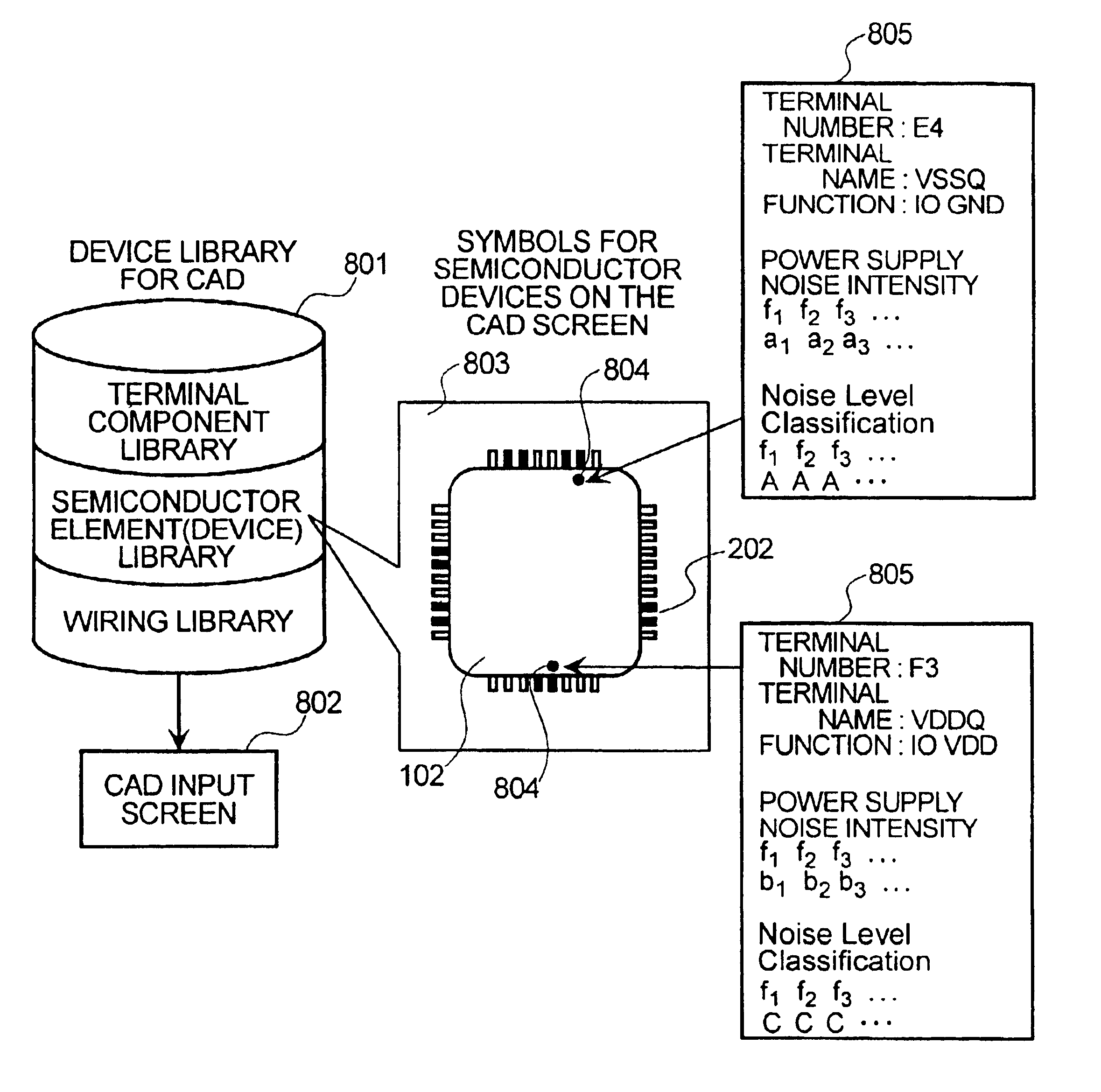
[0068]FIG. 8 depicts a computer aided design (CAD) system having noise level information on the semiconductor device 102 according to one embodiment of the present invention.

[0069]In FIG. 8, a numeral 801 denotes a device library (data base) of terminal components or semiconductor devices for use in designing the substrate layout with a CAD system. A numeral 802 denotes a CAD input screen for performing layout of the substrate 201 using various device symbols from the device library 801. A numeral 803 denotes a semiconductor device symbol that has been selected from the device library 801 and displayed on the CAD input screen 802. A numeral 804 denotes a marking that indicates that a terminal has a high noise level. A numeral 805 denotes terminal information windows providing noise level information (the noise intensity 107 or the noise level classification 301) for the terminals in the semiconductor device symbol 803.

[0070]Traditionally, when the layout CAD is used to perform ...


PUM


Abstract

A semiconductor device includes a semiconductor die having patterned circuitry, a plurality of terminals coupled to the die, and an indication providing signal noise information of at least one of the terminals.

Description

CROSS-REFERENCES TO RELATED APPLICATIONS[0002]The present application is related to and claims priority from Japanese Patent Application No. 2001-277424, filed on Sep. 13, 2001.BACKGROUND OF THE INVENTION[0003]The present invention relates to a semiconductor device and a design support method of an electronic device having the semiconductor device assembled on a substrate or printed circuit board.[0004]At present, data sheets or sales catalog for showing the performance of semiconductor devices, such as microprocessors and LSIs (e.g., ASICs), describe the electric characteristics of the LSIs: (1) absolute rating (FIG. 14); (2) DC characteristics (FIG. 15); and (3) AC characteristics (FIG. 16). In addition, the timing accuracy and delay time for clock and control and bus signals of each of signal terminals are provided to describe the AC characteristics(FIG. 17).[0005]However, the description of EMI (Electro Magnetic Interference) in a substrate packaged with the LSI and in a device ...

Claims


Application Information

Patent Timeline
IPC IPC(8): H01L21/00H01L23/552H05K3/00H05K1/18H05K1/02G06F17/50H01L21/82H01L23/00H01L23/544
CPCH01L23/544H01L21/67282H01L2924/0002H01L23/552H01L2223/54406H01L2223/5442H01L2223/54473H01L2223/54486H01L2924/15311H05K1/0231H05K1/0266H05K1/181H05K3/0005H01L2924/00
Inventor NAKAMURA, SATOSHISUGA, TAKASHINAKAMURA, ATSUSHIYOKOTA, HITOSHIHARA, TSUTOMUUESAKA, KOUICHINOMA, TATSUJITORIGOE, MAKOTO
Owner HITACHI LTD
Why Eureka
Try Eureka