Deformable segmented MEMS mirror

a segmented, mirror technology, applied in the field of adaptive optics, can solve the problems of reducing image quality, difficult control of the shape of the membrane, and corresponding limit of the range of wavefront distortions correctable with the membrane mirror, and achieve the effect of easy control

Inactive Publication Date: 2005-04-05
LUCENT TECH INC
View PDF16 Cites 51 Cited by
  • Summary
  • Abstract
  • Description
  • Claims
  • Application Information

AI Technical Summary

Benefits of technology

The problems in the prior art are addressed, in accordance with the principles of the present invention, by a MEMS device having a deformable segmented mirror. The mirror includes a plurality of movable segments, each segment supported by springs and adjustably positionable offset from a substrate. Each spring is connected at one end to one of the movable segments and at the other end to a stationary plate fixedly offset from the substrate. In one embodiment of the invention, each stationary plate is rigidly attached to a post that supports that plate above the substrate. In a representative embodiment, three springs support each movable segment, and each spring connected to a particular movable segment connects that movable segment to a different respective stationary plate. The MEMS device also has a plurality of electrodes, each of which can be individually biased. A movable segment moves in response to a voltage applied to an electrode located beneath that segment while the springs attached to the segment provide a restoring force when they are stretched from their rest positions by motion of the movable segment to which they are attached. Due to the stationary plates, motion of each movable segment is substantially decoupled from that of the adjacent segments, which makes the shape of the segmented mirror relatively easy to control. In addition, segments in a deformable mirror of the invention can be displaced by a distance that is significantly larger than the maximum deformation amplitude for a membrane mirror of the prior art. The MEMS device can be fabricated using two silicon-on-insulator (SOI) wafers and an etch fabrication technique.

Problems solved by technology

The cumulative effect of these changes along the beam propagation path may lead to beam wandering and spreading and to beam intensity fluctuations, each of which degrades image quality.
However, because each electrode affects the shape of the entire membrane, the shape of the membrane is difficult to control.
In addition, the maximum deformation amplitude for a typical membrane mirror is on the order of 1 μm, which puts a corresponding limit on the range of wavefront distortions correctable with that membrane mirror.

Method used


Image

  • Deformable segmented MEMS mirror
  • Deformable segmented MEMS mirror
  • Deformable segmented MEMS mirror

Examples


Embodiment Construction

Reference herein to “one embodiment” or “an embodiment” means that a particular feature, structure, or characteristic described in connection with the embodiment can be included in at least one embodiment of the invention. The appearances of the phrase “in one embodiment” in various places in the specification are not necessarily all referring to the same embodiment, nor are separate or alternative embodiments mutually exclusive of other embodiments.

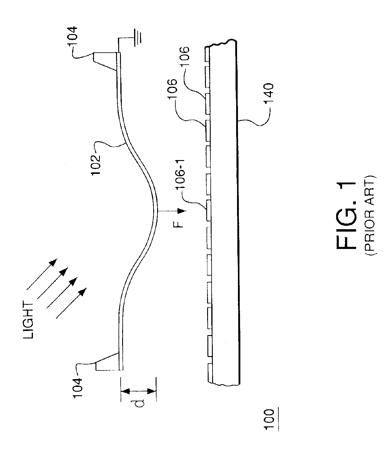
FIG. 1 schematically shows a deformable membrane mirror 100 of the prior art. Mirror 100 includes (i) a deformable membrane 102 mounted on a support structure 104 and (ii) an array of electrodes 106 located beneath membrane 102 on a substrate 140. Each electrode 106 can be individually biased by applying a voltage differential between that electrode and membrane 102 (typically at ground potential). For example, when electrode 106-1 is biased, an attractive electrostatic force (F) is exerted between that electrode and membrane 102 causing...


PUM


Abstract

A MEMS device having a deformable segmented mirror. The mirror includes a plurality of movable segments supported on a substrate using spring vertices, each vertex having a fixed plate and one or more springs. In a representative embodiment, three springs support each movable segment, where each spring connects the movable segment to a different spring vertex. The MEMS device also has a plurality of electrodes, each of which can be individually biased. A movable segment moves in response to a voltage applied to an electrode located beneath that segment while the deformed springs attached to the segment provide a restoring force. Due to the fixed plates, motion of each movable segment is substantially decoupled from that of the adjacent segments, which makes the shape of the segmented mirror relatively easy to control. In addition, segments in a deformable mirror of the invention can be displaced by a distance that is significantly larger than the maximum deformation amplitude for a membrane mirror of the prior art. The MEMS device can be fabricated using two silicon-on-insulator (SOI) wafers and an etch fabrication technique.

Description

BACKGROUND OF THE INVENTION1. Field of the InventionThe present invention relates to adaptive optics and, more specifically, to micro-electromechanical systems (MEMS) for implementing adaptive optics.2. Description of the Related ArtAdaptive optics is a field of optics dedicated to the improvement of optical signals using information about signal distortions introduced by the environment in which the optical signals propagate. An excellent introductory text on the subject is given in “Principles of Adaptive Optics” by R. K. Tyson, Academic Press, San Diego, 1991, the teachings of which are incorporated herein by reference.A representative example of an adaptive optical element is a deformable mirror driven by a wavefront sensor and configured to compensate for atmospheric distortions that affect telescope images. Small naturally occurring variations in temperature (˜1° C.) in the atmosphere cause random turbulent motion of the air and give rise to changes in the atmospheric density ...

Claims


Application Information

Patent Timeline
Patent Type & Authority Patents(United States)
IPC IPC(8): G02B26/06G02B26/00
CPCG02B26/06
Inventor GREYWALL, DENNIS S.
Owner LUCENT TECH INC
Why Eureka
Try Eureka