

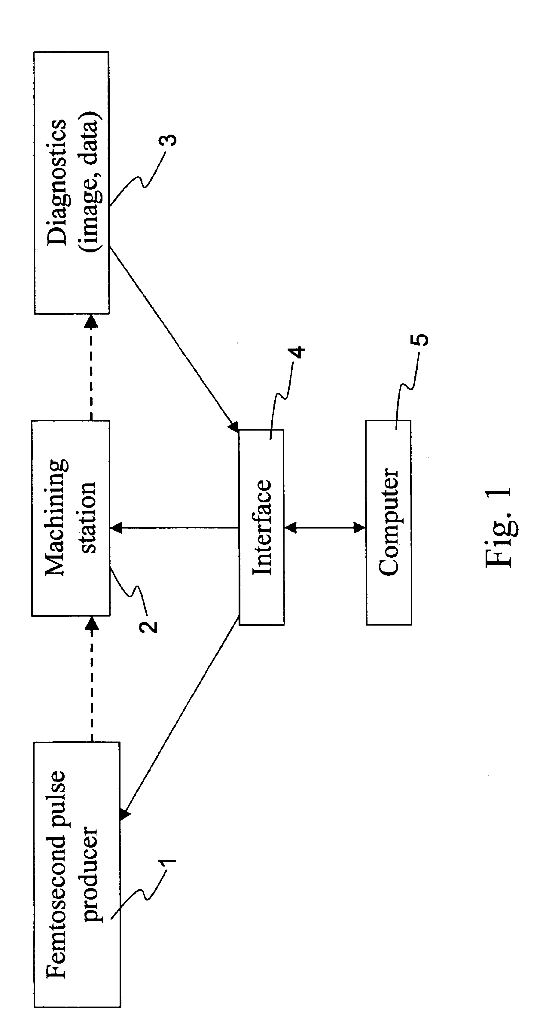
Method and apparatus for repair of defects in materials with short laser pulses
a technology of short laser pulses and repair methods, applied in the field of materials laser repair, can solve the problems of difficult to achieve both, difficulty in achieving both, and the effect of defects not easily identified, and achieve the effect of minimizing peripheral damag
- Summary
- Abstract
- Description
- Claims
- Application Information
AI Technical Summary
Benefits of technology
Problems solved by technology
Method used
Image

Examples
Embodiment Construction
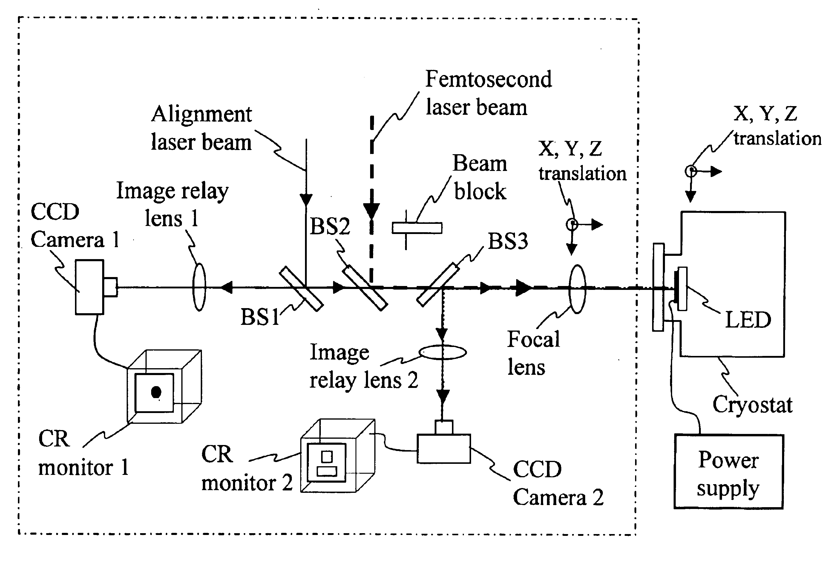
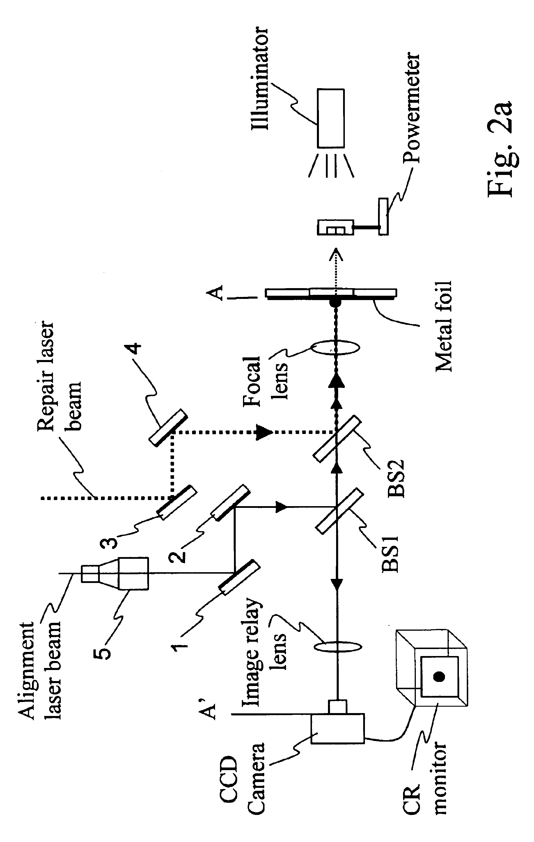
For repairing powered electronic devices, the use of nanosecond lasers is problematic. Because of the relatively large heat-affected zone caused by the deposited energy of a nanosecond laser pulse, plasma effects and unwanted melting are common. These effect areas of the electronic device are collateral to the targeted area and as such, in turn, have a potential to cause further defects. The problems are even more significant when the electronic device is powered. For example, heating of collateral metal leads within an integrated circuit during repair results in some expansion of those leads. The expansion may lead to increased capacitance between leads or to a short there between. If testing of the device is occurring during the repair process, the increased capacitance will change the operating characteristics of the device and may affect device failure. Even more catastrophic is a short which may join two driven lines, power and ground for example, and result in heating of the e...
PUM
| Property | Measurement | Unit |
|---|---|---|
| pulse energy | aaaaa | aaaaa |
| pulse energy | aaaaa | aaaaa |
| optical wavelength | aaaaa | aaaaa |
Abstract
Description
Claims
Application Information