Folded flex circuit interconnect having a grid array interface

a grid array and interconnect technology, applied in the field of electronic packaging, can solve the problems of increasing pitch, increasing the overall density of the array, and often encountering the practicable limit of the array depth, and achieve the effect of increasing the depth of the pad array of the grid array interfa

Inactive Publication Date: 2005-04-12
AVAGO TECH INT SALES PTE LTD
View PDF8 Cites 108 Cited by
  • Summary
  • Abstract
  • Description
  • Claims
  • Application Information

AI Technical Summary

Benefits of technology

In accordance with the invention, a flex circuit-based, grid array interconnect having an increased pad array depth of a grid array interface compared to that of a conventional grid array interconnect is facilitated. Moreover, the flex circuit interconnect in accordance with the invention is well-suited for high frequency signal situations such as, but not limited to, when microstrip and / or coplanar wave guide (CPW) transmission lines are employed to carry signals along the flex circuit interconnect.

Problems solved by technology

Unfortunately in such grid array interconnects, a practical limit to the array depth is often encountered in many cases.
Increasing pitch tends to decrease an overall density of the array.
However, adding layers may greatly increase the cost of the grid array interconnect and may prove impractical or ill advised for certain high frequency applications.
Similarly, increasing a width of the circuit interconnect to allow access to the array from multiple sides may not be permissible in some cases, especially where a space for the grid array interconnect is at a premium.

Method used


Image

  • Folded flex circuit interconnect having a grid array interface
  • Folded flex circuit interconnect having a grid array interface
  • Folded flex circuit interconnect having a grid array interface

Examples


Embodiment Construction

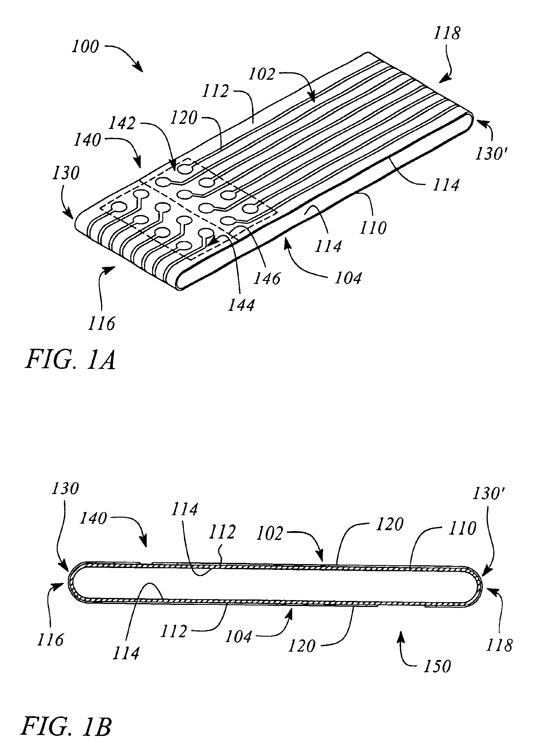
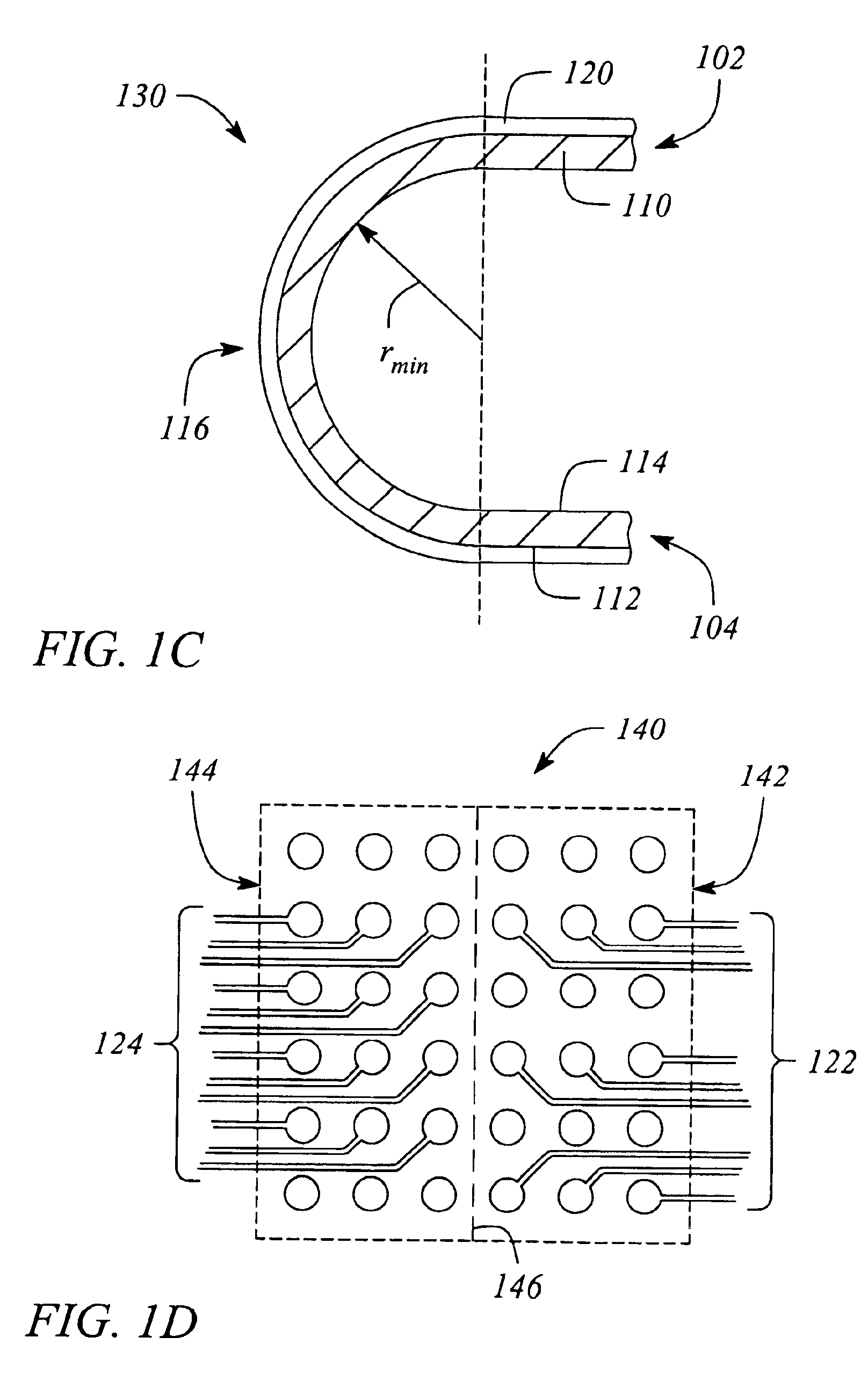
FIG. 1A illustrates perspective view of a folded flex circuit interconnect 100 according to an embodiment in accordance with the invention. FIG. 1B illustrates a side view of the folded flex circuit interconnect 100 that is illustrated in FIG. 1A. The folded flex circuit interconnect 100 of the invention facilitates interconnecting a pair of circuit elements. Moreover, the folded flex circuit interconnect 100 provides for an increase in an achievable array depth of a grid array interface (GAI) of the interconnect 100 compared to a conventional flex circuit interconnect by routing electrical traces from the pad array portion of the GAI in two different sets of traces, each set being routed in an essentially opposite direction. A fold in the folded flex circuit interconnect 100 adjacent to a first side of the pad array essentially changes a direction of one of the sets of traces thereby enabling all of the traces to ultimately travel in a similar direction along the folded flex circui...


PUM


Abstract

A folded flex circuit interconnect increases a number of interconnection pads of a grid array interface available to accommodate high count outputs from distinct circuit elements. The circuit interconnect includes a substrate capable of being folded, a conductor layer adjacent to a surface of the substrate, and a pad array having an interconnection pad connected to the conductor layer at a first end of the circuit interconnect. The pad array is part of the grid array interface. An optics module includes the folded flex circuit interconnect and an optical unit. The folded flex circuit interconnect further includes an electrical interface at a second end that is connected to the conductor layer. The folded flex circuit interconnect connects to the optical unit using the electrical interface. The circuit interconnect connects the optical unit to a motherboard using the pad array at the first end.

Description

TECHNICAL FIELDThe invention relates to electronic packaging. In particular, the invention relates to high density electronic interconnects using grid arrays.BACKGROUND ARTA grid array interface (GAI) is used as a means for interfacing or connecting high-density integrated circuits (ICs) and / or other high pin-out electronic components or modules to a carrier circuit or to a circuit interconnect in many modern high-density electronic packaging applications. Additionally, GAIs are employed to connect a circuit interconnect to a carrier circuit and occasionally to connect components to components. Examples of such GAIs include, but are not limited to, a ball grid array (BGA) and a pin grid array (PGA). An example of a carrier circuit includes a printed circuit board (PCB) while an example of a circuit interconnect includes a flexible, multi-conductor, interconnect, known as a ‘flex’ circuit. The GAI provides a high-density, parallel electrical interface between essentially any pair of ...

Claims


Application Information

Patent Timeline
Patent Type & Authority Patents(United States)
IPC IPC(8): G02B6/42H05K1/18H05K1/14H01L21/60
CPCG02B6/4201H05K1/189H05K1/141H05K1/147H05K2201/056H01L2924/0002H05K2201/10734H01L2924/00G02B6/4281G02B6/4283
Inventor ROSENAU, STEVEN A.ALI, MOHAMMED E.LEMOFF, BRIAN E.WINDOVER, LISA A.
Owner AVAGO TECH INT SALES PTE LTD
Why Eureka
Try Eureka