

Device manufacturing method, device manufactured thereby and a mask for use in the method
a manufacturing method and device technology, applied in the direction of printers, instruments, photographic processes, etc., can solve the problems of overlay errors, unsuitable material for refractive optical elements at euv wavelengths, and illumination at an angl
- Summary
- Abstract
- Description
- Claims
- Application Information
AI Technical Summary
Benefits of technology
Problems solved by technology
Method used
Image

Examples
Embodiment Construction
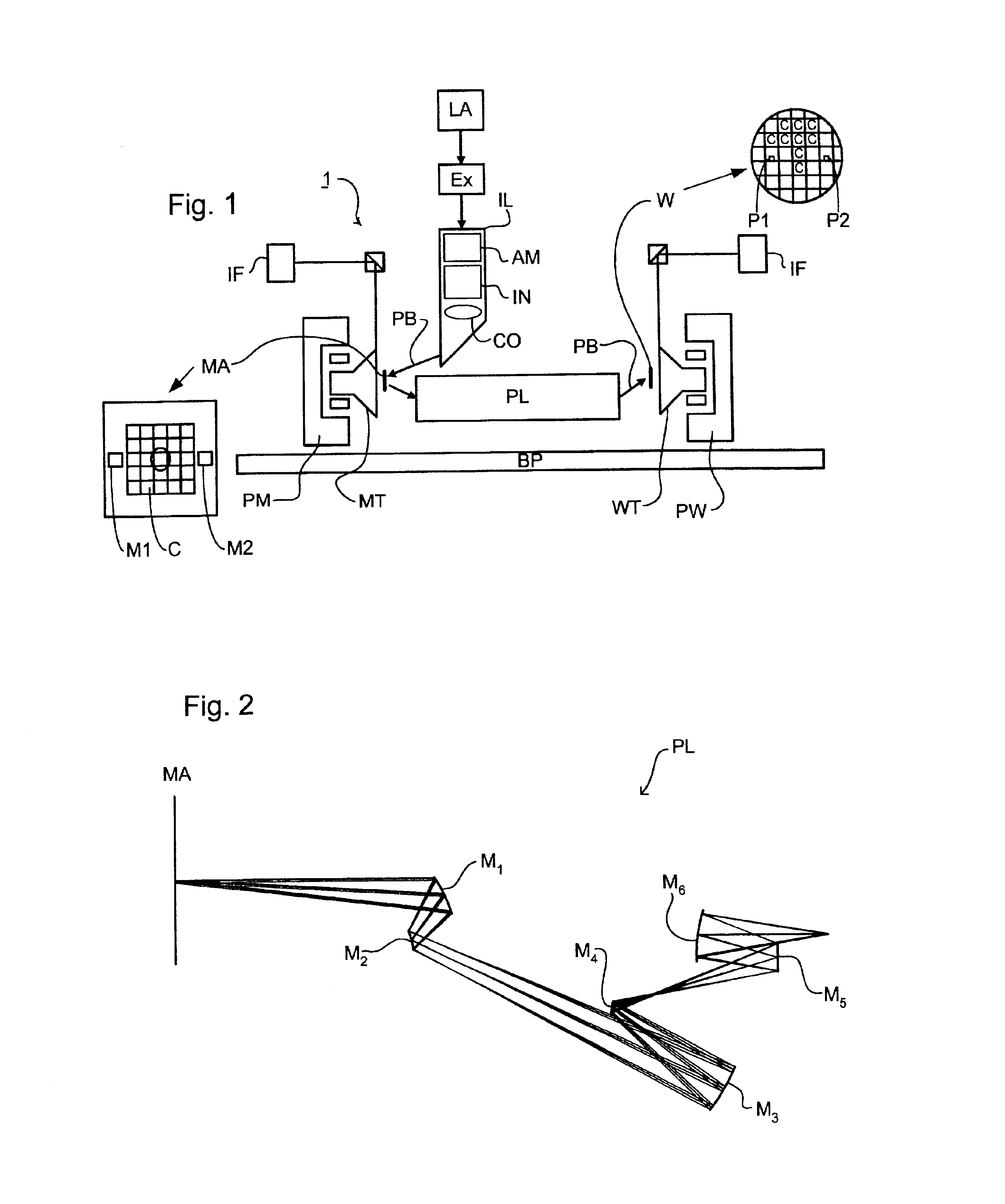
y the projection system; and
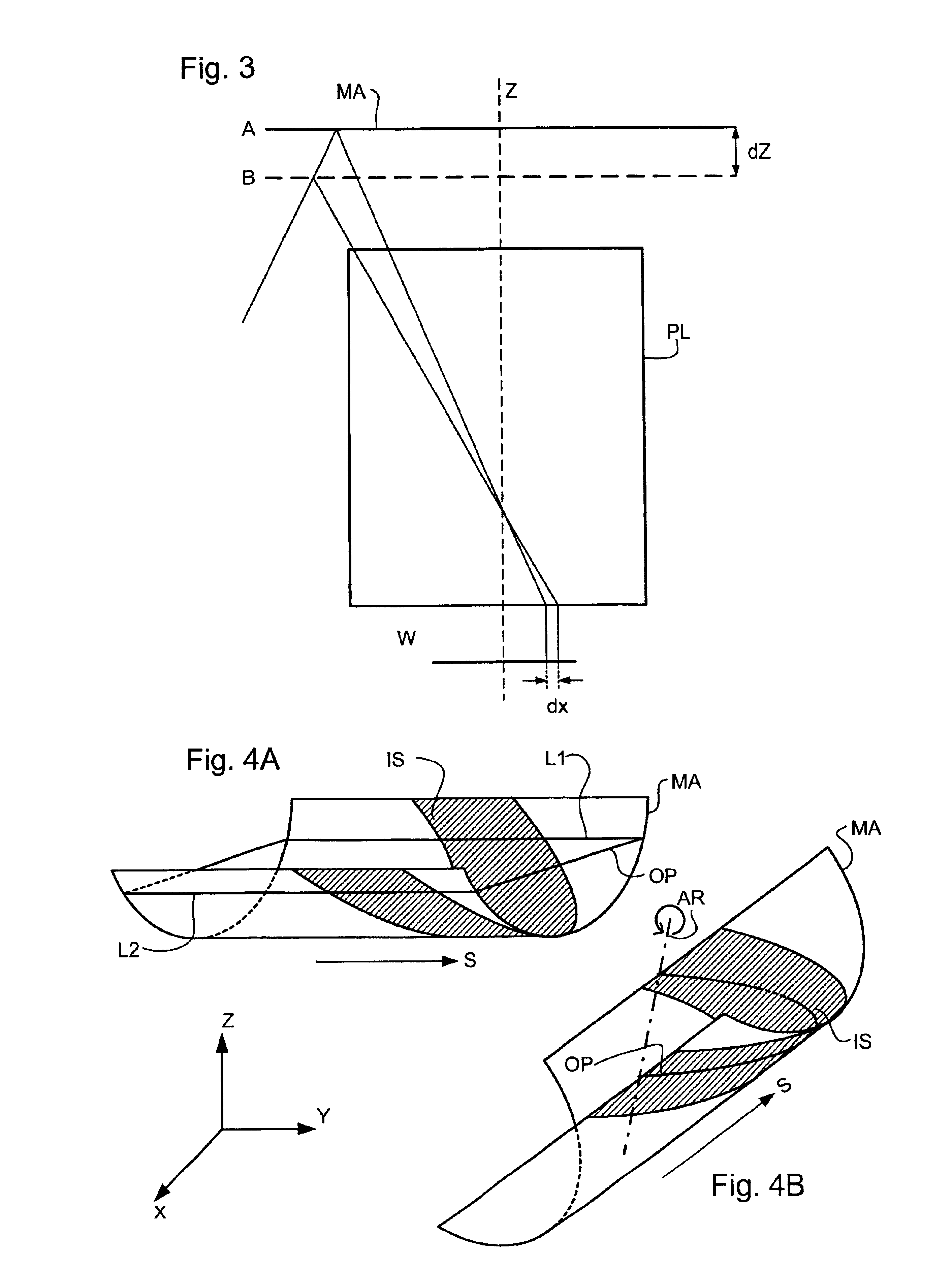
[0026]FIGS. 4A and B illustrate effects of rotation of the mask;
[0027]FIG. 5 is a diagram illustrating a technique of measuring the vertical position of a reflective mask having a transparent substrate;
[0028]FIG. 6 is a diagram showing the position of markers used in an alternative technique for measuring the vertical position of the mask; and
[0029]FIGS. 7 to 12 are diagrams illustrating the effects of different deformations of the mask on the image projected on the substrate.
[0030]In the Figures, corresponding reference symbols indicate corresponding parts.
DETAILED DESCRIPTION
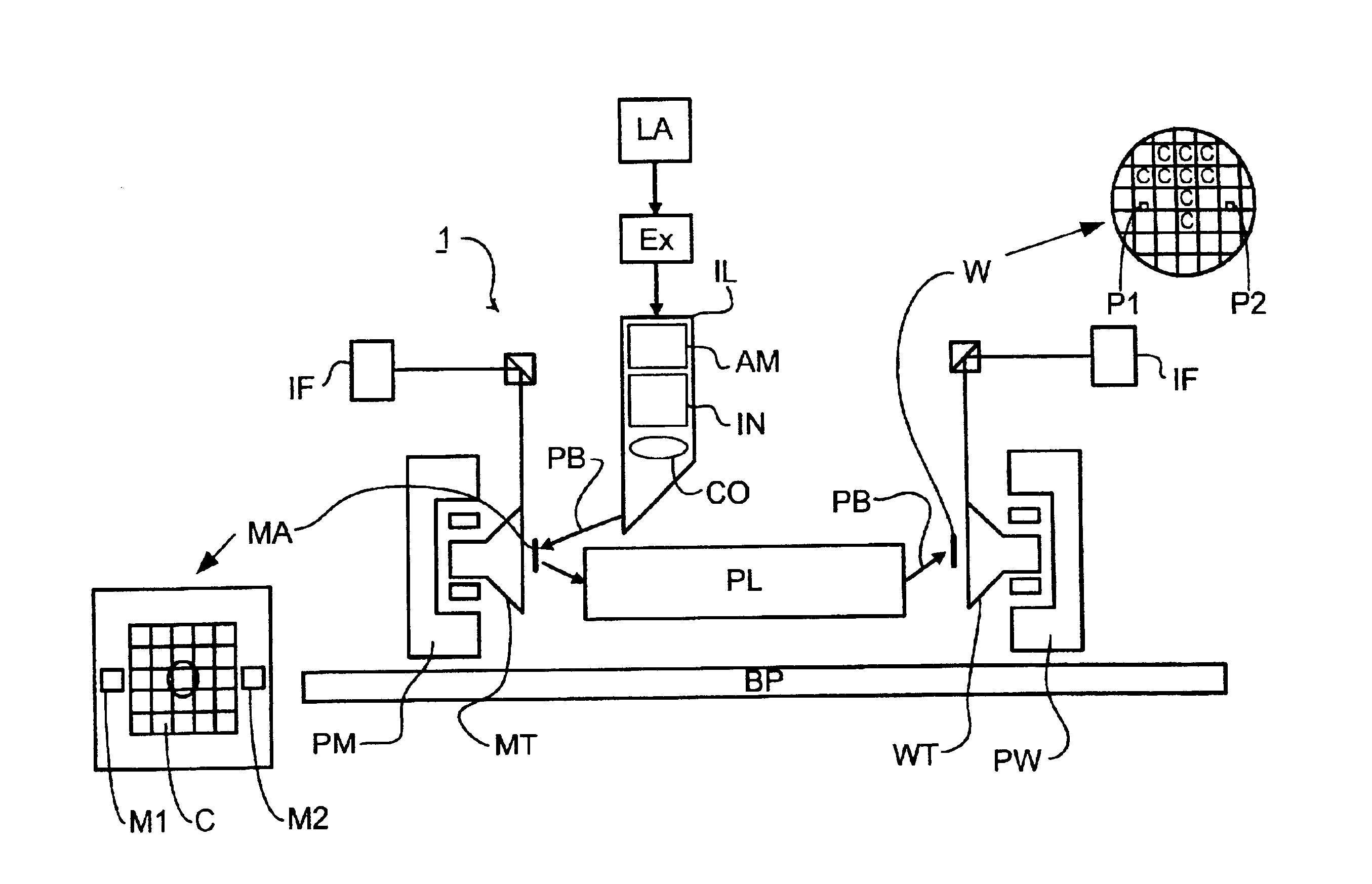
[0031]FIG. 1 schematically depicts a lithographic projection apparatus according to one embodiment of the invention. The apparatus comprises:
[0032]A radiation system Ex, IL, for supplying a projection beam PB of radiation (e.g. EUV radiation). In this particular example, the radiation system also comprises a radiation source LA;
[0033]A first object table (mask table) MT provided wit...
PUM
 Abstract
Description
Claims
Application Information