Folded interposer

a technology of interposer and folding plate, which is applied in the direction of solid-state devices, printed circuit aspects, basic electric elements, etc., can solve the problems of reducing requiring large amounts of memory in a much smaller electronic device, and affecting the overall size of the package, so as to reduce the unused or wasted space, the effect of efficient stacking

Inactive Publication Date: 2005-04-26
MICRON TECH INC
View PDF26 Cites 136 Cited by
  • Summary
  • Abstract
  • Description
  • Claims
  • Application Information

AI Technical Summary

Benefits of technology

[0023]The present invention relates to a folded interposer and a high density semiconductor package that utilizes the folded interposer. The folded interposer is comprised of a thin, flexible material that can be folded around one or multiple semiconductor dice. The folded interposer allows multiple semiconductor dice to be efficiently stacked in a high density semiconductor package by reducing the unused or wasted space between stacked semiconductor dice. The present invention also relates to a method of packaging semiconductor dice in a high density arrangement and a method of forming the high density semiconductor die package. Finally, the present invention relates to a computer system that incorporates the folded interposer in a high density semiconductor die package.

Problems solved by technology

Consumers want their portable devices to perform the same functions as their desktop computers, therefore requiring large amounts of memory in a much smaller electronic device.
However, these packages are ill-suited for use in small, portable electronic devices because they inefficiently use their real estate, which unnecessarily adds to the overall size of the package.
This multichip module is not suited for small electronic devices because the adhesive layer between the dice increases the overall thickness of the semiconductor package.
Since the shelves are rigid and provide space between the chips, the packaging scheme is not suited for use in small electronic devices.
This separation adds to the overall thickness of the integrated circuit package, making it incompatible for use in electronic devices that require small semiconductor packages.
Since the column-like connections cause unused space between the substrates, this semiconductor package is incompatible with electronic devices that require small semiconductor packages.
While numerous high density semiconductor packages exist, they share a common disadvantage in that they inefficiently use the space of the semiconductor package.
The unused or wasted space may be the result of thick adhesive layers between semiconductor dice or may be caused by rigid interposers or other spacers.
Small electronic devices, such as cell phones and PDAs, have very limited space and cannot afford to waste any of this space.
Reducing the wasted or unused space in a semiconductor die package is essential because large packages occupy too much of this limited space.
Over time, these heat cycles place a large amount of mechanical stress on the electrical contacts and solder connections between the semiconductor die and substrate.
After repeated cycles, the contacts and connections may fail.
However, this severely limits the types of components that can be used together.

Method used


Image

  • Folded interposer
  • Folded interposer
  • Folded interposer

Examples


Embodiment Construction

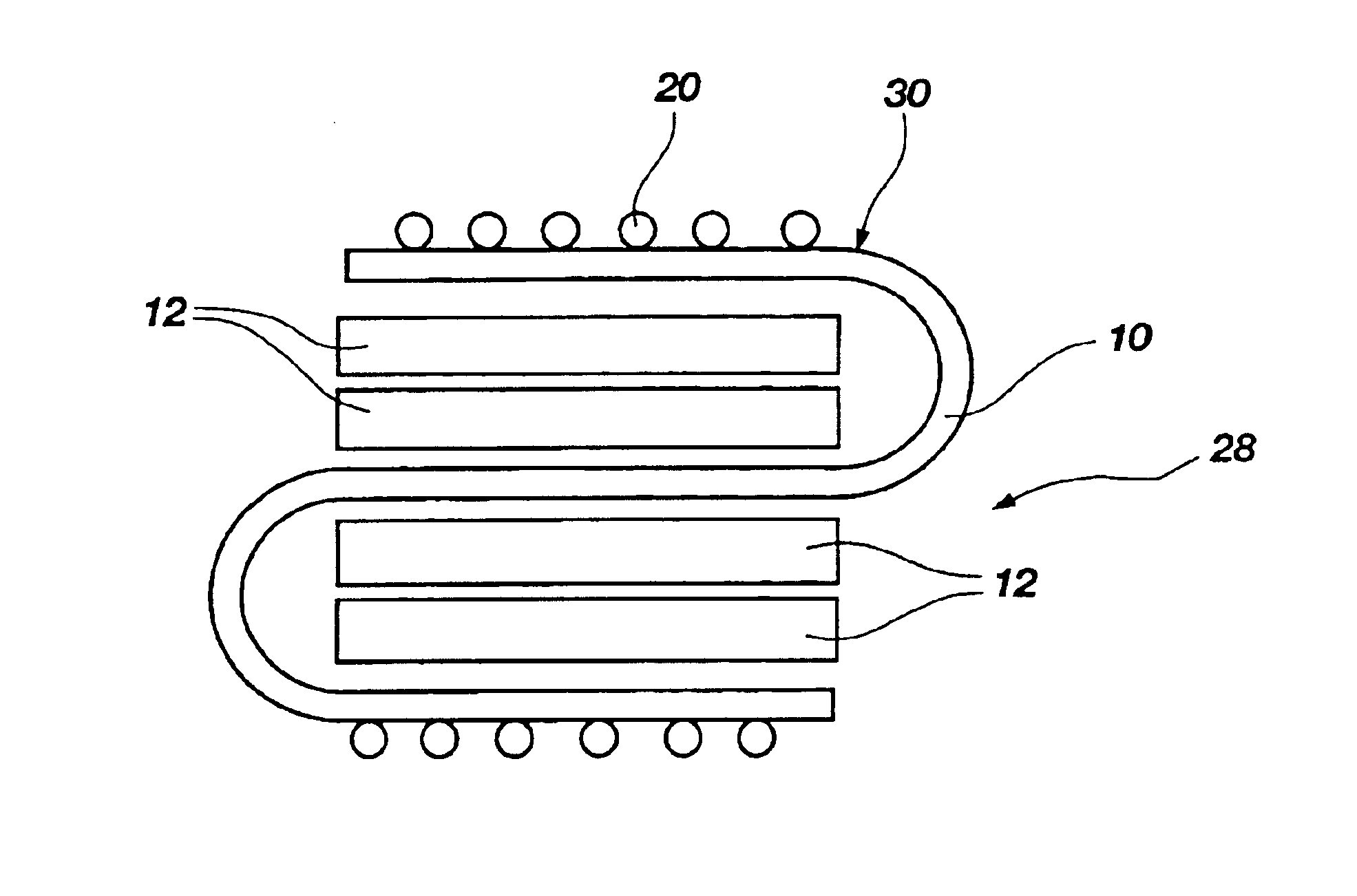
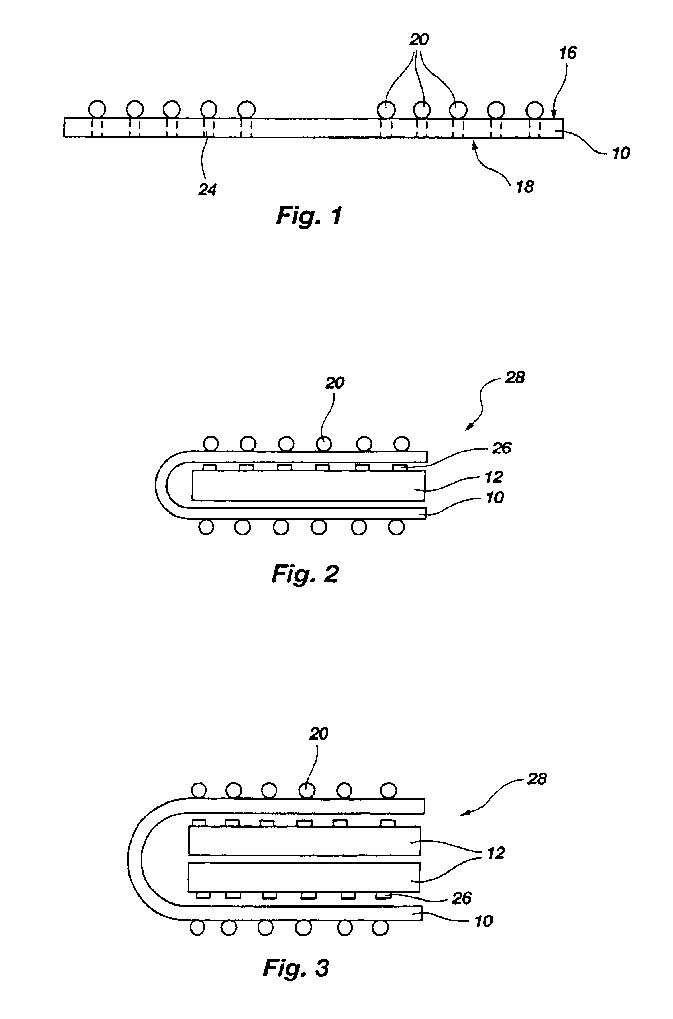
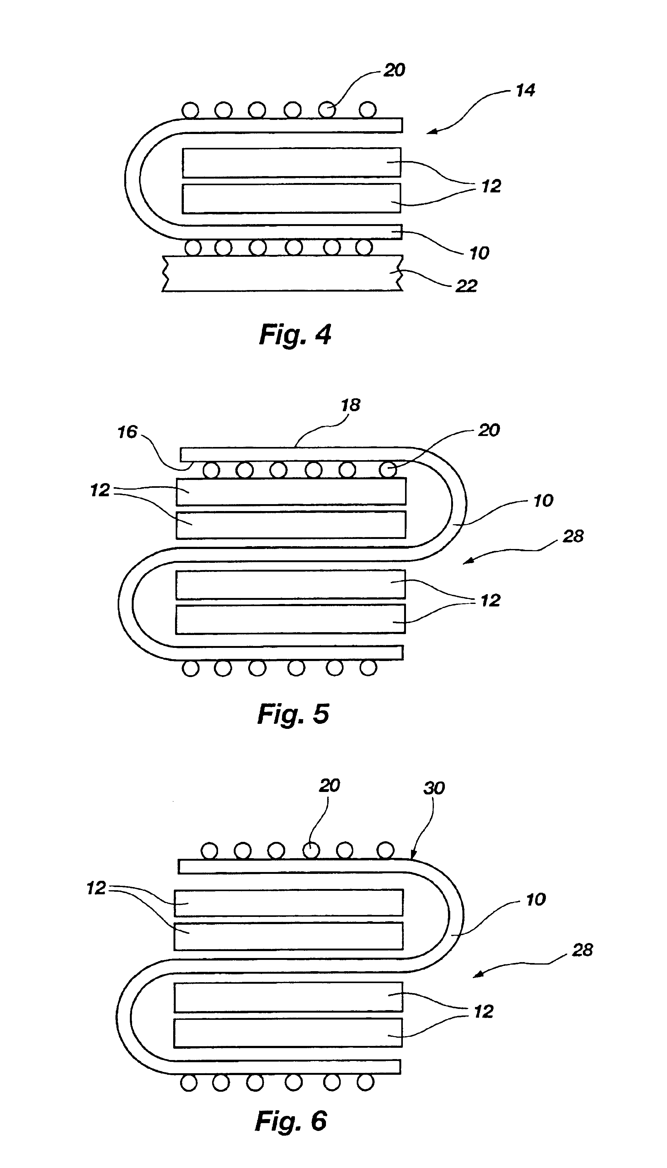
[0031]Illustrated in drawing FIG. 1 is an interposer 10, which includes a first surface 16 and a second surface 18. The first surface 16 includes electrical contacts 20 for attaching the interposer 10 to a substrate (not shown), such as a printed circuit board. Vias 24 extend through the interposer 10 from the first surface 16 to the second surface 18 and are in communication with the electrical contacts 20. The folded interposer 10 is comprised of a thin, flexible material, such as an insulative polymer. The material has substantially the same width as a semiconductor die so that the material covers the surface of the semiconductor die. Preferably, the material should also be thermally conductive to allow for adequate dissipation of heat generated by the electrical circuitry.

[0032]As illustrated in drawing FIGS. 2 and 3 the interposer 10 is flexible enough to fold around one or multiple semiconductor dice 12. Preferably, the semiconductor dice 12 are bare, unpackaged die. As is ill...


PUM


Abstract

A folded interposer used to achieve a high density semiconductor package is disclosed. The folded interposer is comprised of a thin, flexible material that can be folded around one or multiple semiconductor dice in a serpentine fashion. The semiconductor dice are then attached to a substrate through electrical contacts on the interposer. The folded interposer allows multiple semiconductor dice to be efficiently stacked in a high density semiconductor package by reducing the unused or waster space between stacked semiconductor dice. Vias extending through the folded interposer provide electrical communication between the semiconductor dice and the substrate. The present invention also relates to a method of packaging semiconductor dice in a high density arrangement and a method of forming the high density semiconductor package.

Description

BACKGROUND OF THE INVENTION[0001]1. Field of the Invention[0002]The present invention relates to a semiconductor die package. More particularly, the present invention relates to a folded interposer used to increase the semiconductor die density of a high density semiconductor package.[0003]2. Background of Related Art[0004]As electronic devices, such as cell phones and personal digital assistants (“PDAs”), become smaller, more portable, and more technologically advanced, there is an increasing need for high density semiconductor die packages that can provide the necessary memory for these devices. New, high density semiconductor packages must be easily and cheaply manufactured with existing equipment. In addition, the package must maintain the reliability and quality of the semiconductor die. A semiconductor die package contains many electrical circuit components that must be interconnected to form functional, integrated circuits.[0005]Consumers want their portable devices to perfor...

Claims


Application Information

Patent Timeline
Patent Type & Authority Patents(United States)
IPC IPC(8): H01L23/52H01L23/538H01L25/065
CPCH01L23/4985H01L23/5387H01L25/0657H05K1/147H01L2224/16H01L2225/06579H05K2201/10378H01L2225/06517
Inventor LARSON, CHARLES E.
Owner MICRON TECH INC
Why Eureka
Try Eureka