Methods of incorporating germanium within CMOS process

a technology of germanium and cmos, applied in the direction of basic electric elements, electrical equipment, semiconductor devices, etc., can solve the problems of ineffective germane-deposition catalysis on the son surface, layer wicking,

Inactive Publication Date: 2005-05-03
CISCO TECH INC
View PDF4 Cites 124 Cited by
  • Summary
  • Abstract
  • Description
  • Claims
  • Application Information

AI Technical Summary

Benefits of technology

[0010]Advantageously, with the insertion of one or more Ge layers, the present invention provides the capability of converting an optical signal carried at a wavelength range that can be absorbed by the germanium into an electrical signal.

Problems solved by technology

The growth of this layer wick occurs only on the opening in the SON mask because the germane-deposition catalysis on the SON surface is not effective.

Method used


Image

  • Methods of incorporating germanium within CMOS process
  • Methods of incorporating germanium within CMOS process
  • Methods of incorporating germanium within CMOS process

Examples


first embodiment

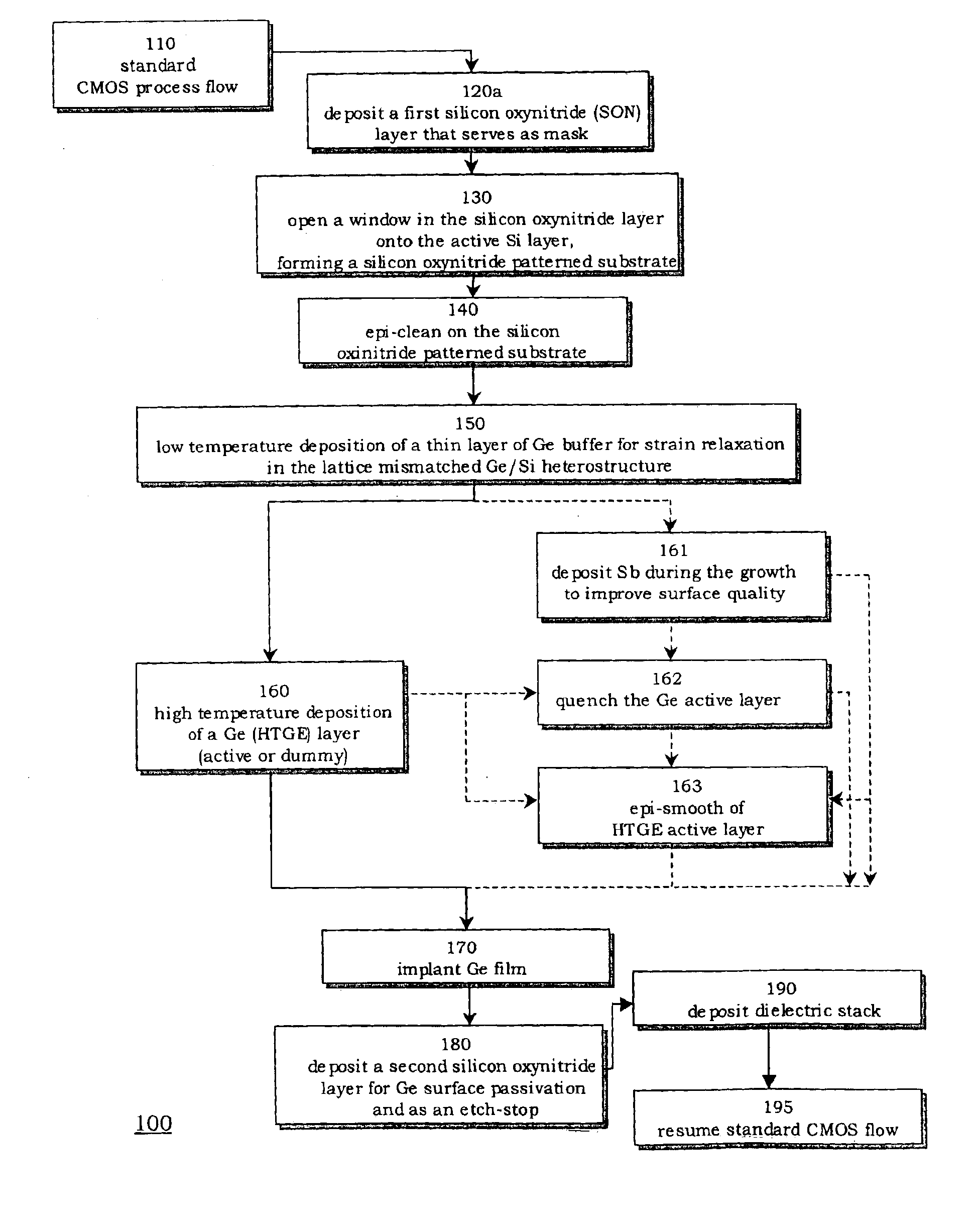
[0014]Referring now to FIG. 1, therein is shown a flow diagram illustrating the process 100 for incorporating germanium growth in a standard CMOS process. In step 110, the manufacturing of a chip employs a standard CMOS flow with a silicon substrate. The process 100 continues until the highest temperature step, typically the salicide annealing, is performed. In step 120, the process 100 deposits a first silicon oxynitride layer. Step 120 is typically a conventional CMOS process step. One of ordinary skill in the art should recognize that the deposition of one or more silicon oxynitride layers is typical in a CMOS process. Similar or various types of compositions of silicon oxynitride can be practiced without departing from the spirit of the present invention. The first oxynitride layer is then patterned in order to expose areas of the underlying Si substrate in the process step 130. One embodiment illustrating the present invention includes depositing the silicon oxynitride layer by...

second embodiment

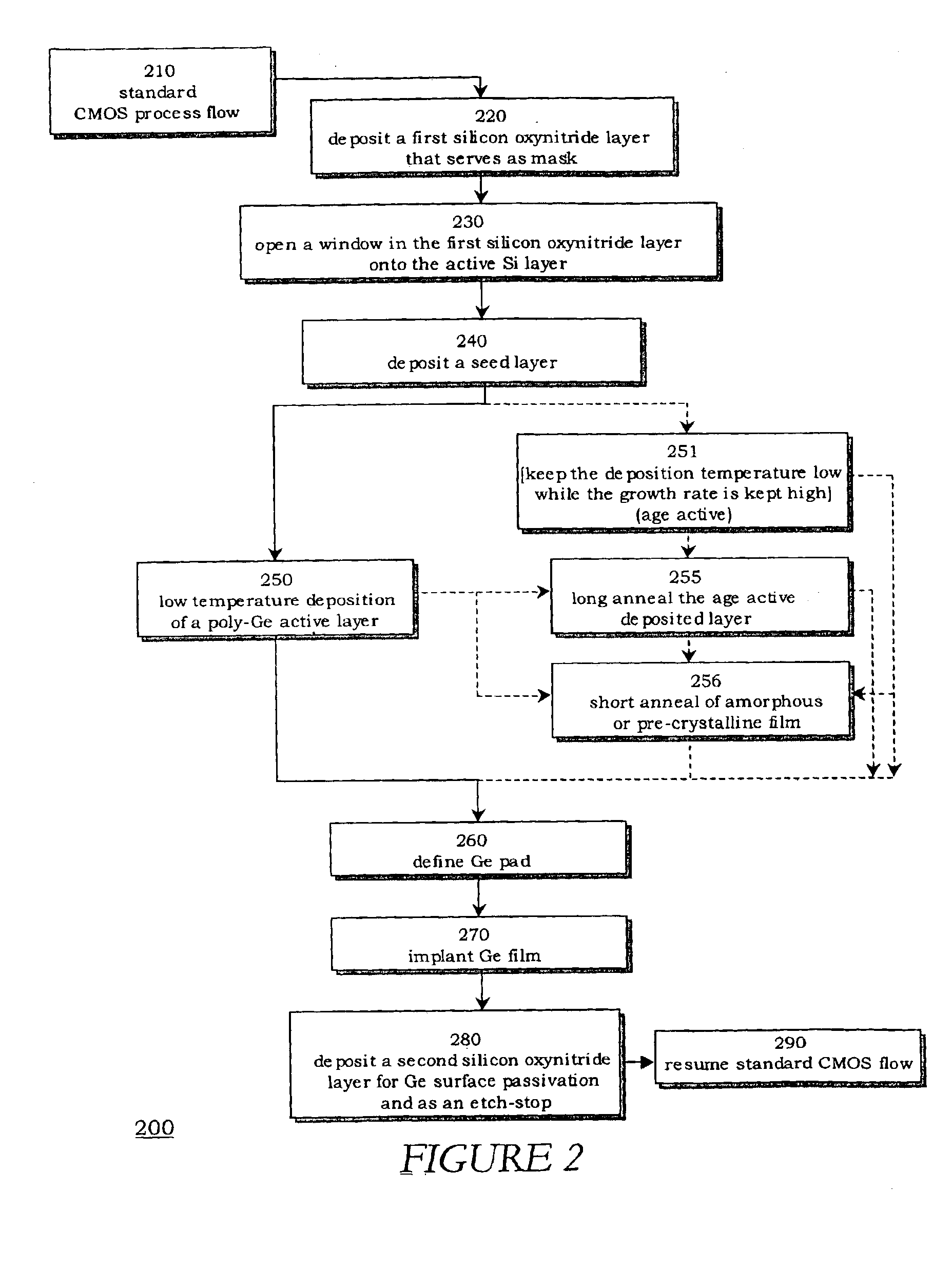
[0031]In FIG. 2, therein is shown a flow diagram illustrating a process for poly-Ge growth. At step 210, the manufacturing of a chip employs a standard CMOS flow with a silicon substrate using a silicon-on-insulator process. The process 200 continues until the salicide annealing. In step 220, the process 200 deposits a first silicon oxynitride layer. This oxynitride layer is then patterned in order to expose areas of the underlying Si substrate in the process step 230.

[0032]At step 230, the process 200 opens a window in the first silicon oxynitride layer onto the active silicon layer. This step defines the opening to the active Si substrate. The substrate can be n-doped. The active window shape created in step 230 is optimized considering photonic design requirements. A standard, ex-situ wet etching / cleaning step is performed prior to sample loading in the reactor where the subsequent process step will take place. An in-situ high-temperature step is optional.

[0033]The process 200 de...


PUM


Abstract

Methods for deposition of a Ge layer during a CMOS process on a monolithic device are disclosed. The insertion of the Ge layer enables the conversion of light to electrical signals easily. As a result of this method, standard metals can be attached directly to the Ge in completing an electrical circuit. Vias can also be used to connect to the Ge layer. In a first aspect of the invention, a method comprises the step of incorporating the deposition of Ge at multiple temperatures in a standard CMOS process. In a second aspect of the invention, a method comprises the step of incorporating the deposition of poly-Ge growth in a standard CMOS process.

Description

[0001]This application claims priority from U.S. Provisional Application Ser. No. 60 / 389,962, filed on Jun. 19, 2002, U.S. Provisional Application Ser. No. 60 / 391,277, filed on Jun. 24, 2002, U.S. Provisional Application Ser. No. 60 / 393,484, filed on Jul. 3, 2002, U.S. Provisional Application Ser. No. 60 / 432,946, filed on Dec. 12, 2002, U.S. Provisional Application Ser. No. 60 / 432,925, filed on Dec. 12, 2002, and U.S. Provisional Application Ser. No. 60 / 433,470, filed on Dec. 13, 2002.BACKGROUND INFORMATION[0002]1. Field of the Invention[0003]The invention relates generally to the field of chip manufacturing process, and is more particularly to fabrication with one or more germanium layers.[0004]2. Description of Related Art[0005]The convergence of silicon and optical fabrication processes presents an attractive manufacturing solution by leveraging the use of a standard CMOS (complementary metal-oxide semiconductor) manufacturing process. Some optical companies have selected III-V s...

Claims


Application Information

Patent Timeline
Patent Type & Authority Patents(United States)
IPC IPC(8): H01L21/70H01L21/8238
CPCH01L21/8238H01L21/823878Y10S438/958
Inventor GUNN, III, LAWRENCE C.CAPELLINI, GIOVANNIRATTIER, MAXIME JEANPINGUET, THIERRY J.
Owner CISCO TECH INC
Why Eureka
Try Eureka