Self aligned metal interconnection and method of making the same

a self-aligning, metal interconnection technology, applied in the direction of digital transmission, transmission, basic electric elements, etc., can solve the problems of inability to reliably form holes, difficulty in forming via holes and trenches of upper conductive layers, and difficulty in forming via sidewalls that do not permit effective electrical conta

Inactive Publication Date: 2005-05-03
MONTEREY RES LLC
View PDF2 Cites 8 Cited by
  • Summary
  • Abstract
  • Description
  • Claims
  • Application Information

AI Technical Summary

Problems solved by technology

In this first technique, the second etching that forms the via hole and the upper conductive layer trench is difficult, since the greater the aspect ratio (i.e., height to width) of the hole, the less reliably the hole is formed.
6(b)), and result in a via sidewall slope that does not permit effective electrical contact between the resulting via and the underlying conductive layer (see FIG.
Proper alignment becomes more and more difficult as the size of the structures becomes smaller and smaller, and effective via openings may be quite difficult to produce at a width of 0.18 μm and smaller.

Method used


Image

  • Self aligned metal interconnection and method of making the same
  • Self aligned metal interconnection and method of making the same
  • Self aligned metal interconnection and method of making the same

Examples


Embodiment Construction

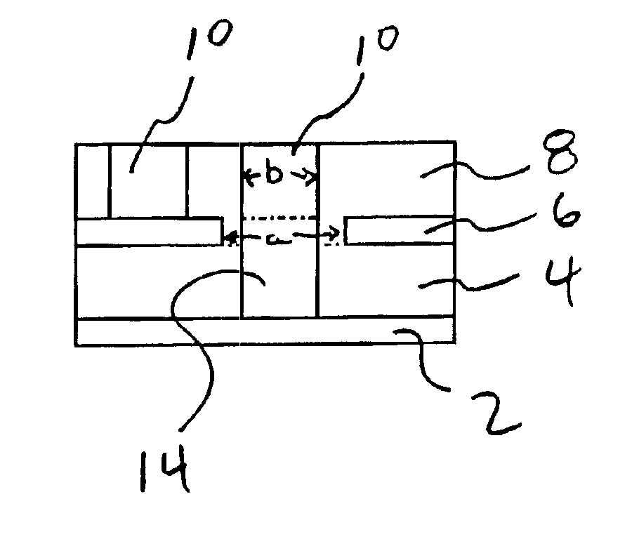
[0026]FIG. 13 is a view from above of an embodiment of an interconnecting structure of the present invention. Illustrated are a lower conductive layer 2, electrically connected to an upper conductive layer 10 by a via 14 which has one end in contact with the lower conductive layer, and the other end in contact with the upper conductive layer. The upper conductive layer is in-laid into an upper dielectric layer 8. In the present invention, the via has a cross section of a rectangle, preferably a rectangle having axes of unequal length. In the illustration, the portion of the upper and lower conductive layers are shown in the pattern of a wire, but any overall pattern is possible. For example, the lower conductive layer may comprise a “landing pad” portion or section to which a via may be connected, roughly corresponding to a portion or section of a wire having an expanded width relative to other portions or sections of the lower conductive layer that will not be electrically connecte...


PUM

PropertyMeasurementUnit
widthaaaaaaaaaa
dimensionaaaaaaaaaa
conductiveaaaaaaaaaa

Abstract

A method of making a structure, includes filling a via hole with a conductive material, to form a via. The via hole passes through an etch-stop opening. In both directions along a first axis dielectric material is present between the via hole and edges of the etch-stop layer, and in both directions along a second axis, perpendicular to said first axis, dielectric material is not present between the via hole and edges of the etch-stop layer.

Description

CROSS REFERENCE TO RELATED APPLICATIONS[0001]This application is a continuation of, and claims the benefit of the earlier filing date of, U.S. patent application Ser. No. 09 / 595,630, filed 15 Jun. 2000, now abandoned the disclosure of which is expressly incorporated herein.BACKGROUND[0002]The present invention relates to interconnection structures, including interlevel interconnection structures, devices containing these structures, and methods of making these structures and devices.[0003]Typically, interconnection structures between conductive layers in an integrated circuit are known as contacts or vias (hereinafter “vias”), which are typically metallic structures that have ends in electrical contact with the conductive, layers. The vias are typically formed by depositing a dielectric layer over a first conductive layer, etching a hole through the dielectric layer, filling the holes with a conductor material to form the vias (and optionally, the overlying conductive layer), then e...

Claims


Application Information

Patent Timeline
Patent Type & Authority Patents(United States)
IPC IPC(8): H01L21/768H01L23/522H01L23/532
CPCH01L21/7681H01L23/53295H01L23/5226H01L2924/0002H01L2924/00
Inventor BLOSSE, ALAIN
Owner MONTEREY RES LLC
Why Eureka
Try Eureka