Lateral DMOS transistor having reduced surface field

a technology surface field, which is applied in the direction of semiconductor devices, semiconductor/solid-state device details, electrical apparatus, etc., can solve the problems of deteriorating the reliability of lateral dmos transistor, significant reduction of high electric field, and deteriorating the reliability of the devi

Inactive Publication Date: 2005-05-03
SEMICON COMPONENTS IND LLC
View PDF1 Cites 25 Cited by
  • Summary
  • Abstract
  • Description
  • Claims
  • Application Information

AI Technical Summary

Problems solved by technology

A common drawback of the FIG. 1 transistor is the high electric field present at the corner of p-type top region 15 near n+-type drain region 17.
However, this structure does not result in any significant reduction in the high electric field.
This high electric field at the interface between the silicon layer and oxid

Method used


Image

  • Lateral DMOS transistor having reduced surface field
  • Lateral DMOS transistor having reduced surface field
  • Lateral DMOS transistor having reduced surface field

Examples


Embodiment Construction

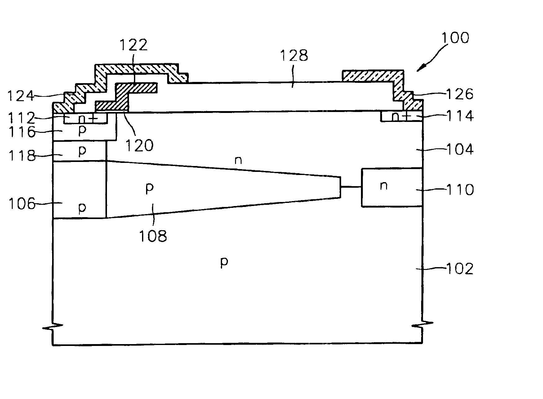
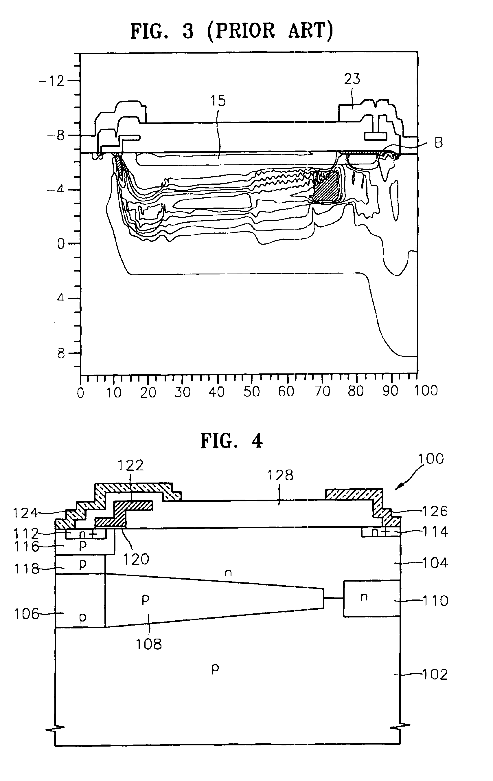
[0037]FIG. 4 is a sectional view of a lateral double diffused metal oxide semiconductor (DMOS) transistor 100 according to an embodiment of the present invention. Lateral DMOS transistor 100 includes an n-type drift region 104 formed on a p-type silicon substrate 102. A first p-type bottom layer 106, a second p-type bottom layer 108, and an n-type buried layer 110 are formed along the interface between p-type silicon substrate 102 and n-type drift region 104. The first and second p-type bottom layers 106 and 108 abut each other laterally, and second p-type bottom layer 106 is spaced laterally from n-type buried layer 110 a predetermined distance. The upper and lower surfaces of second p-type bottom layer 108 contact n-type drift region 104 and p-type silicon substrate 102, respectively.

[0038]N+-type drain region 114 is formed along the surface of n-type drift region 104. N+-type source region 112 is formed in a p-type body region 116 which is in turn formed in n-type drift region 10...


PUM


Abstract

In accordance with the present invention, a metal oxide semiconductor (MOS) transistor has a substrate of a first conductivity type. A drift region of a second conductivity type is formed over the substrate. A body region of the first conductivity type is formed in the drift region. A source region of the second conductivity is formed in the body region. A gate extends over a surface portion of the body region and overlaps each of the source region and the body region such that the surface portion of the body region forms a channel region of the transistor. A drain region of the second conductivity type is formed in the drift region. The drain region is laterally spaced from the source region a first predetermined distance. A first buried layer of the first conductivity type extends into the substrate and the drift region. The first buried layer laterally extends between the source and drain regions.

Description

CROSS-REFERENCES TO RELATED APPLICATIONS[0001]This application claims priority to Korean patent application number 2002-7528, filed Feb. 8, 2002, which is incorporated herein by reference.BACKGROUND OF THE INVENTION[0002]The present invention relates to a lateral double diffused metal oxide semiconductor (DMOS) transistor, and more particularly, to a lateral DMOS transistor having reduced surface field (RESURF).[0003]In general, a breakdown voltage of a lateral DMOS transistor is closely related to the thickness of an epitaxial layer. For example, when the thickness of the epitaxial layer is reduced, the breakdown voltage of the lateral DMOS transistor is reduced. Nowadays, a lateral DMOS transistor having a thin epitaxial layer and a high breakdown voltage can be fabricated by using RESURF technology.[0004]FIG. 1 is a sectional view of a conventional lateral DMOS transistor 10. Lateral DMOS transistor 10 has an n-type drift region 12 formed on a p-type silicon substrate 11. A p-typ...

Claims


Application Information

Patent Timeline
IPC IPC(8): H01L29/76H01L23/58H01L29/66H01L29/772H01L31/0264H01L31/101H01L29/94H01L31/062H01L31/06H01L31/0328H01L31/113H01L21/266H01L21/336H01L21/74H01L29/08H01L29/10H01L29/78
CPCH01L29/7801H01L29/1095H01L29/66674H01L29/1083H01L21/266H01L21/74H01L29/0847H01L29/7816H01L29/7835H01L29/0878H01L29/402H01L29/772
Inventor JEON, CHANG-KIKIM, MIN-HWANKIM, SUNG-LYONG
Owner SEMICON COMPONENTS IND LLC
Why Eureka
Try Eureka