Lithographic template and method of formation and use

a template and lithographic technology, applied in the field of lithographic templates, can solve the problems of the number of required steps for fabricating the template, masking and etching steps, and the conventional resist, masking and etching process

Inactive Publication Date: 2005-05-10
NXP USA INC +1
View PDF6 Cites 50 Cited by
  • Summary
  • Abstract
  • Description
  • Claims
  • Application Information

AI Technical Summary

Problems solved by technology

Certain problems exist though with this SFIL template fabrication methodology.
In particular, problems exist with the conventional resist, masking and etch process.
More particularly, problems exist with respect to the number of required steps needed to fabricate the template, namely, the etching of the chrome, the etching of the quartz material, and the required etch and resist removal steps.
In addition, there exist problems with respect to electron-beam writing of the template and the inspection of the template subsequent to fabrication.
In addition, inspectability is not readily achievable due to the template being comprised of a single material.

Method used


Image

  • Lithographic template and method of formation and use
  • Lithographic template and method of formation and use
  • Lithographic template and method of formation and use

Examples


first embodiment

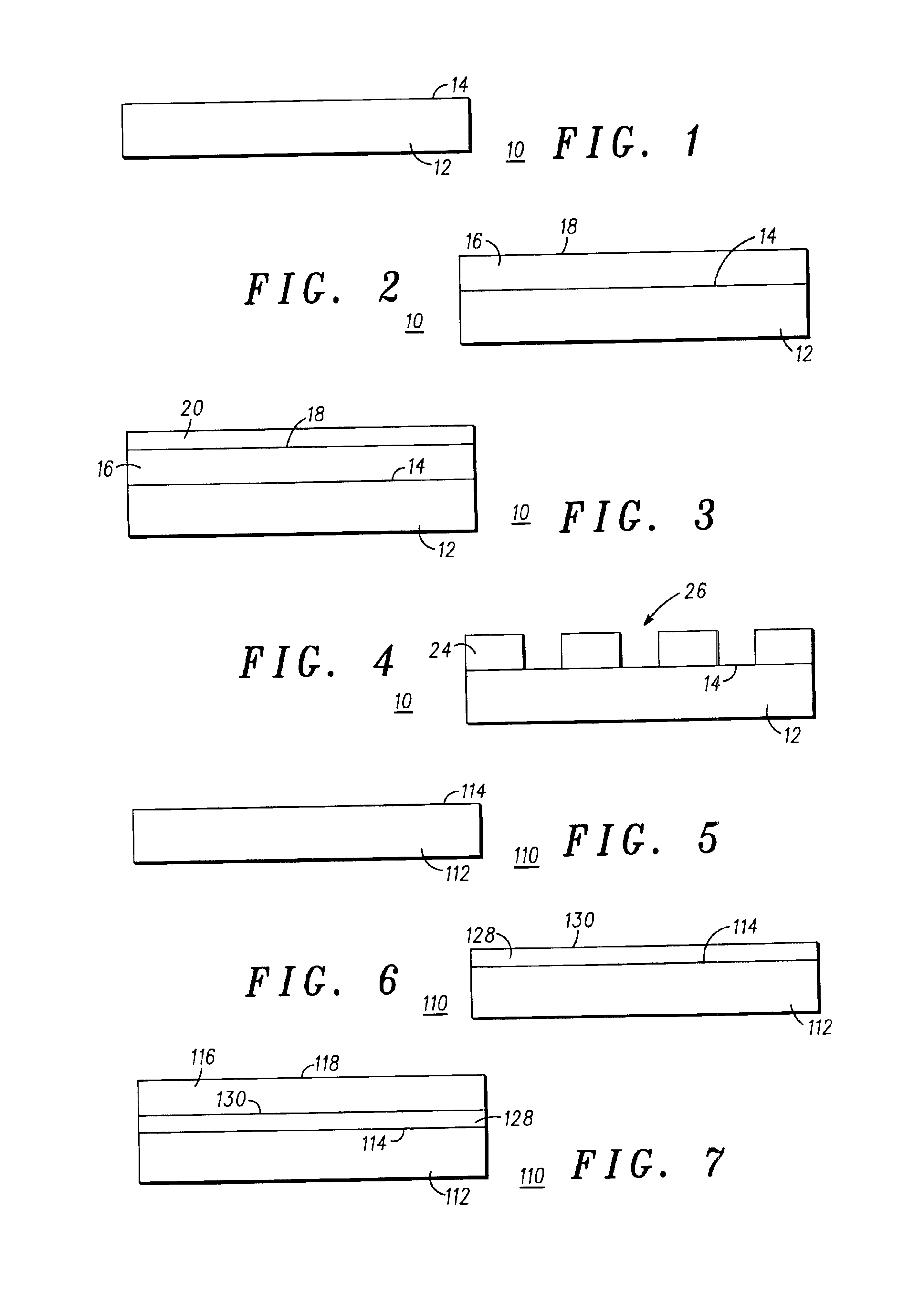
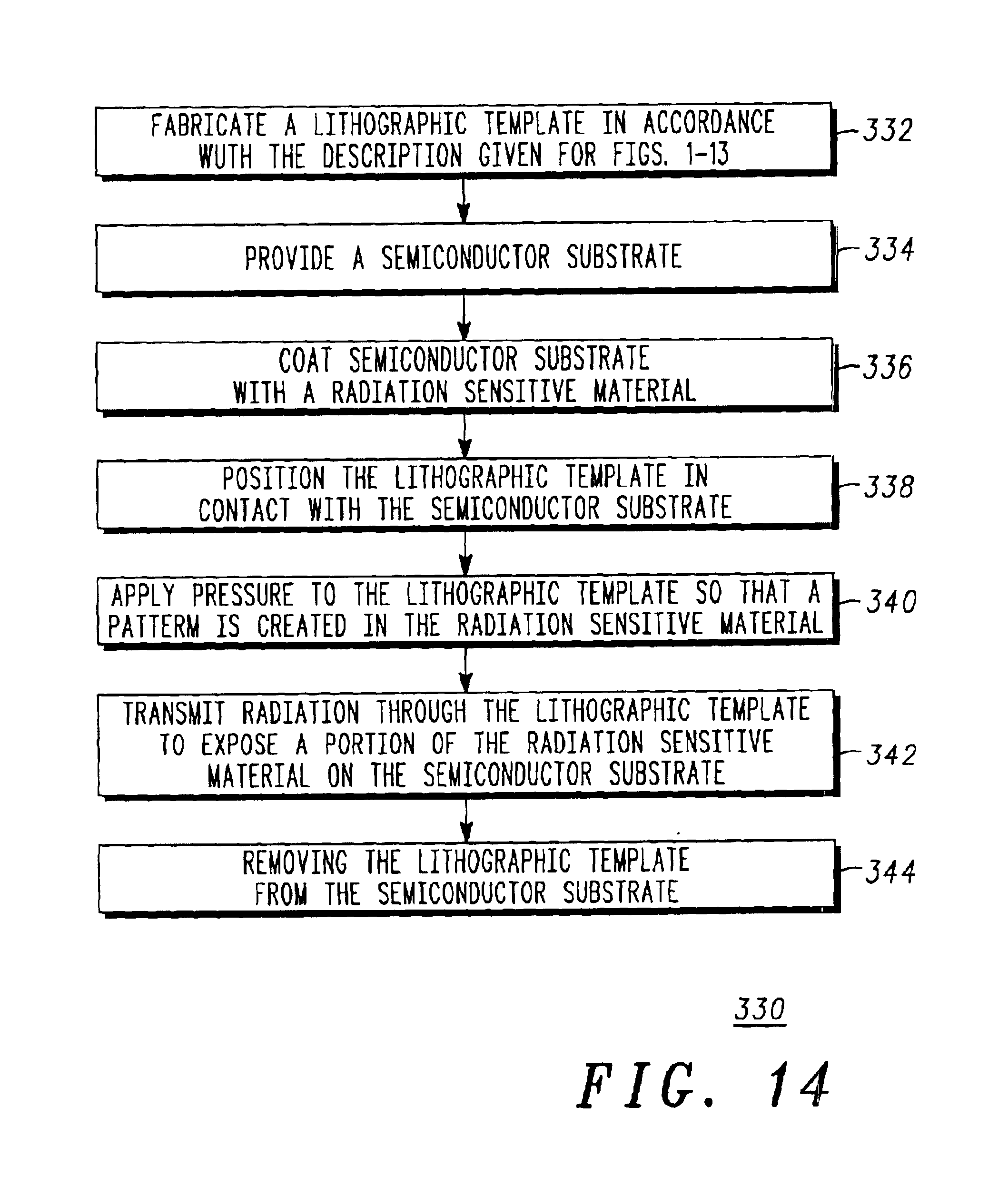
[0022]Referring to FIGS. 1-13, illustrated in cross-sectional views, are a plurality of process steps for fabricating a lithographic template according to the preferred embodiments of the present invention. Referring more specifically to FIGS. 1-4, illustrated are the steps in the process of fabricating the lithographic template according to the present invention.

[0023]Referring now to FIG. 1, illustrated is a first step in the process of fabricating a lithographic template 10 according to the present invention. Illustrated is substrate 12, having a surface 14. Substrate 12 is disclosed as being comprised of a transparent or semi-transparent material, such as a quartz material, a polycarbonate material, a pyrex material, a calcium fluoride (CaF2) material, a magnesium fluoride material (MgF2), or any other similar type of material, that is transparent or semi-transparent to light.

[0024]Referring now to FIG. 2, illustrated is substrate 12, having deposited thereon uppermost surface 1...

second embodiment

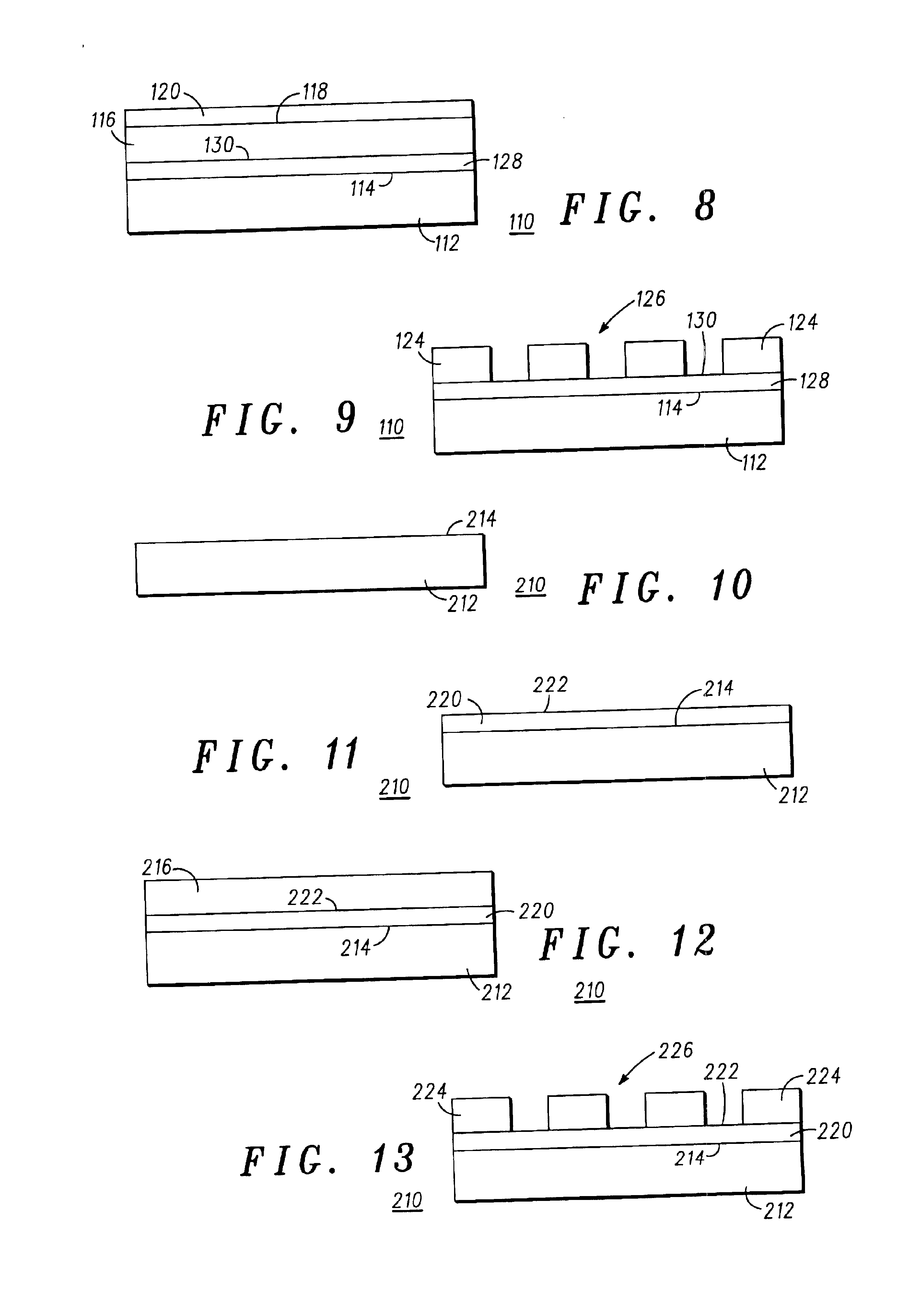
[0033]Referring now to FIGS. 5-9, illustrated are the steps in the process of fabricating the lithographic template according to the present invention in which a separate contrast enhancement layer (discussed presently) is included, sandwiched between substrate 12 and patterning layer 16. More specifically, referring to FIG. 5, illustrated is a first step In the process of fabricating a lithographic template 110 according to the present invention. Illustrated is substrate 112, having a surface 114. Substrate 112 is disclosed as being comprised of a transparent or semi-transparent material, such as a quartz material, a polycarbonate material, a pyrex material, a calcium fluoride (CaF2) material, a magnesium fluoride material (MgF2), or any other similar type of material, that is transparent to light.

[0034]Referring now to FIG. 6, illustrated is substrate 112, having deposited thereon surface 114, a contrast enhancement layer 128. Contrast enhancement layer 128 is disclosed as being f...

third embodiment

[0041]Referring now to FIGS. 10-13, illustrated are the steps in the process of fabricating the lithographic template according to the present invention. More specifically, referring now to FIG. 10, illustrated is a first step in the process of fabricating a lithographic template 210 according to the present invention. Illustrated is substrate 212, having a surface 214. Substrate 212 is disclosed as being comprised of a transparent or semi-transparent material, such as a quartz material, a polycarbonate material, a pyrex material, a calcium fluoride (CaF2) material, a magnesium fluoride material (MgF2), or any other similar type of material, that is transparent or semi-transparent to light.

[0042]Referring now to FIG. 11, illustrated is substrate 212, having deposited thereon surface 214 and a charge dissipation layer 220. Charge dissipation layer 220 is disclosed as being formed of a transparent or semi-transparent conducting oxide. Examples of transparent or semi-transparent conduc...


PUM

PropertyMeasurementUnit
thickaaaaaaaaaa
thicknessaaaaaaaaaa
thicknessaaaaaaaaaa

Abstract

This invention relates to a lithographic template, a method of forming the lithographic template and a method for forming devices with the lithographic template. The lithographic template (10, 110, 210) is formed having a substrate (12, 112, 212) and a charge dissipation layer (20, 120, 220), and a patterned imageable relief layer, (16, 116, 216) formed on a surface (14, 114, 214) of the substrate (10, 110, 210) using radiation. The template (10, 110, 210) is used in the fabrication of a semiconductor device (344) for affecting a pattern in the device (344) by positioning (338) the template (10, 11, 210) in close proximity to semiconductor device (344) having a radiation sensitive material (334) formed thereon and applying a pressure (340) to cause the radiation sensitive material to flow into the relief image present on the template (10, 110, 210). Radiation (342) is then applied through the template (10, 110, 210) to cure portions of the radiation sensitive material and define the pattern in the radiation sensitive material. The template (10, 110, 210) is then removed to complete fabrication of semiconductor device (344).

Description

FIELD OF THE INVENTION[0001]The present invention relates to semiconductor devices, microelectronic devices, micro-electro mechanical devices, photonic, optoelectronic, and microfluidic devices, and more particularly to a lithographic template, a method of forming the lithographic template and a method for forming these devices with the lithographic template.BACKGROUND OF THE INVENTION[0002]The fabrication of integrated circuits involves the creation of several layers of materials that interact in some fashion. One or more of these layers may be patterned so various regions of the layer have different electrical characteristics, which may be interconnected within the layer or to other layers to create electrical components and circuits. These regions may be created by selectively introducing or removing various materials. The patterns that define such regions are often created by lithographic processes. For example, a layer of photoresist material is applied onto a layer overlying a...

Claims


Application Information

Patent Timeline
Patent Type & Authority Patents(United States)
IPC IPC(8): G03F7/09G03F7/00
CPCB82Y10/00B82Y40/00G03F7/093G03F7/0017G03F7/0002
Inventor MANCINI, DAVID P.RESNICK, DOUGLAS J.WILLSON, CARLTON GRANT
Owner NXP USA INC
Why Eureka
Try Eureka