Optimized electronic package

a technology of electronic packaging and integrated circuits, applied in the direction of semiconductor devices, semiconductor/solid-state device details, electrical apparatus, etc., can solve the problems of first solder, second solder connection , premature failure, affecting both product cost (lower yield) and reliability, and achieves a relatively low cost, increased yield, and prevent the effect of solder connection cracking

Inactive Publication Date: 2005-05-17
IBM CORP
View PDF13 Cites 17 Cited by
  • Summary
  • Abstract
  • Description
  • Claims
  • Application Information

AI Technical Summary

Benefits of technology

[0009]It is another object of this invention to provide an electronic package that will be manufactured in such a manner that has increased yields and can be produced at a relatively lower cost than many current products.
[0010]It is yet another object of the invention to provide an electronic package that substantially prevents cracking of a solder connection between a ground layer and ground plane of the electronic package and a printed circuit board.

Problems solved by technology

These handling, assembly, and CTE stresses can cause first solder connection 35 and / or second solder connection 39 to prematurely fail affecting both product cost (lower yields) and reliability.

Method used


Image

  • Optimized electronic package
  • Optimized electronic package
  • Optimized electronic package

Examples


Embodiment Construction

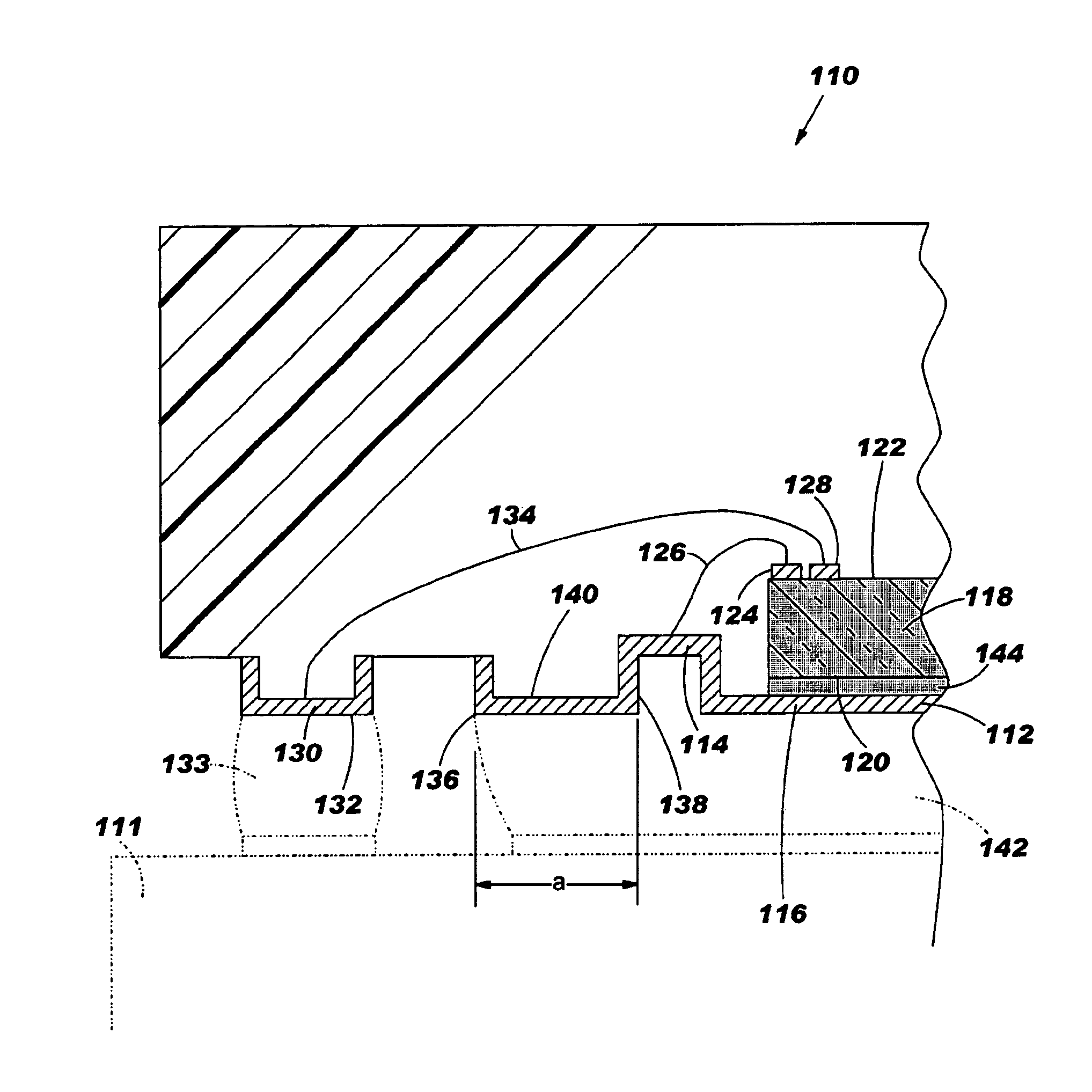
[0024]A portion of electronic package 110 for use with a printed circuit board 111 (shown in phantom) illustrating one embodiment of the present invention is shown in FIG. 2A. FIG. 2A shows a much enlarged view, in elevation, of a portion of electronic package 110 taken along line 2A—2A in FIG. 2B. FIG. 2B shows a bottom view of the portion of electronic package 110 shown in FIG. 2A. Referring to FIG. 2A, electronic package 110 includes a ground layer 112 having an upper section 114 and a lower section 116. The electronic package 110 includes a semiconductor chip 118 having a first surface 120 and a second surface 122, the first surface on and electrically coupled to lower section 116 of ground layer 112. The second surface 122 of semiconductor chip 118 includes a first conductive pad 124 wirebonded by wire 126 to upper section 114 of ground layer 112 and a second conductive pad 128. A conductive signal layer 130, comprising a plurality of conductive signal pads 131 (see FIG. 2B), i...


PUM


Abstract

An electronic package for use with a printed circuit board is provided. The electronic package includes a ground layer having an upper and lower section, a semiconductor chip, a conductive signal layer and a ground plane having a first section electrically connected to the upper section of the ground layer and a second section substantially planar with said lower section of said ground layer, the second section of the ground plane having an additional area to prevent cracking of a solder connection between the ground layer, the ground plane and the printed circuit board.

Description

TECHNICAL FIELD[0001]This invention relates to an electronic package for use in packaging semiconductors, and more particularly to such packages where an electronic device (e.g. semiconductor chip) is located on a substrate and coupled thereto.BACKGROUND OF THE INVENTION[0002]Electronic packages are widely used in a variety of well-known applications from computers to computer controls of a wide variety of devices, for example, automobiles and home appliances, among others. Electronic packages for complex systems typically are comprised of interconnected integrated circuit chips. The integrated circuit chips are usually made from a semiconductor material such as silicon or gallium arsenide. Microscopic circuits are formed in the various layers of the integrated circuit chips using known photolithographic techniques. The integrated circuit chips may be mounted in a package which may then mounted on a printed circuit board. Electronic packages including integrated circuit chips typica...

Claims


Application Information

Patent Timeline
Patent Type & Authority Patents(United States)
IPC IPC(8): H01L23/495H01L23/48H01L23/28H01L23/31H01L23/12H01L21/60H01L23/00H01L23/49H01L23/498H01L23/50
CPCH01L23/49548H01L23/49816H01L23/50H01L23/562H01L24/48H01L23/3107H01L2224/48253H01L2924/01033H01L2224/32245H01L2924/30107H01L2924/15311H01L2924/14H01L2924/10329H01L2924/0781H01L2924/014H01L2924/01082H01L2924/01079H01L2924/01047H01L2924/01046H01L2924/01031H01L24/45H01L24/83H01L2224/45144H01L2224/48091H01L2224/48247H01L2224/48257H01L2224/484H01L2224/48599H01L2224/73265H01L2224/83801H01L2924/01004H01L2924/01005H01L2924/01006H01L2924/01014H01L2924/01015H01L2924/0102H01L2924/01028H01L2924/00014H01L2924/00H01L2924/3512H01L2924/181H01L2924/1815H01L2924/351H01L2924/00012H01L2224/85399H01L2224/05599
Inventor AWAD, ELIEMALONEY, JOHN J.
Owner IBM CORP
Why Eureka
Try Eureka