Methods of forming backside connections on a wafer stack

a backside connection and stack technology, applied in the field of wafer bonding, can solve the problems of poor electrical connection formation, negative affecting device performance, and reducing production yields

Inactive Publication Date: 2005-05-24
TAHOE RES LTD
View PDF15 Cites 100 Cited by
  • Summary
  • Abstract
  • Description
  • Claims
  • Application Information

AI Technical Summary

Problems solved by technology

The misalignment between vias 113 and the conductors 115 of interconnect structure 114 may cause poor electrical connections to be formed between the conductors 115 and the conductive material 118 in vias 113, which can negatively affect device performance and lower production yields.

Method used


Image

  • Methods of forming backside connections on a wafer stack
  • Methods of forming backside connections on a wafer stack
  • Methods of forming backside connections on a wafer stack

Examples


Embodiment Construction

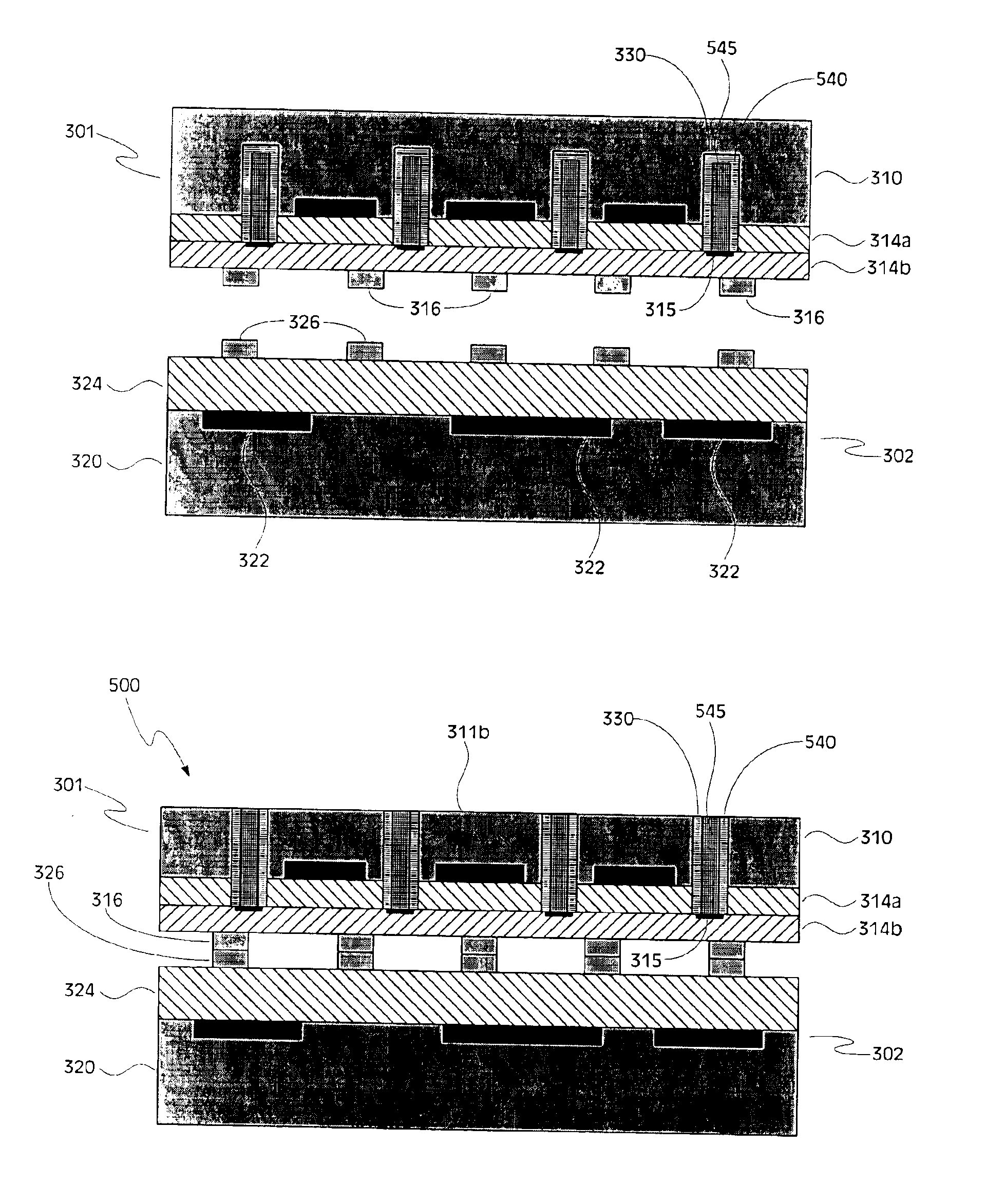
[0016]Disclosed are embodiments of a method of forming backside connections on a wafer stack. In the disclosed embodiments, vias for backside connections are formed from a wafer's front side prior to bonding with a second wafer, and misalignment of the vias resulting from an inability to achieve adequate registration between features formed on opposing sides of the wafer is, therefore, minimized. Various embodiments of this method of forming backside connections on a wafer stack are disclosed in the block diagrams of FIGS. 2, 4A-4B and 6A-6B, respectively.

[0017]Turning now specifically to FIG. 2, illustrated is an embodiment of a method 200 of forming backside connections on a wafer stack. The embodiments of the method 200 shown in FIG. 2 are further illustrated in the schematic diagrams of FIGS. 3A through 3M, and reference should be made to these figures as called out in the text.

[0018]Referring initially to FIGS. 3A and 3B, a first wafer 301 is illustrated. A plan view of the waf...


PUM


Abstract

Various methods of forming backside connections on a wafer stack are disclosed. To form the backside connections, vias are formed in a first wafer that is to be bonded with a second wafer. The vias used for the backside connections are formed on a side of the first wafer along with an interconnect structure, and the backside connections are formed on an opposing side of the first wafer using these vias.

Description

FIELD OF THE INVENTION[0001]The invention relates generally to wafer bonding and, more particularly, to methods of forming backside connections on a wafer stack.BACKGROUND OF THE INVENTION[0002]Wafer bonding is the joining together of two or more semiconductor wafers upon which integrated circuitry has been formed to form a three-dimensional wafer stack. The wafer stack is subsequently diced into separate “stacked die,” each stacked die having multiple layers of integrated circuitry. Wafer stacking technology offers a number of potential benefits, including improved form factors, lower costs, enhanced performance, and greater integration through “system-on-chip” solutions. System-on-chip (SOC) architectures formed by wafer stacking can enable high bandwidth connectivity of products—e.g., logic circuitry and dynamic random access memory (DRAM)—that otherwise have incompatible process flows. There are many applications for wafer stacking technology, including high performance processi...

Claims


Application Information

Patent Timeline
Patent Type & Authority Patents(United States)
IPC IPC(8): H01L25/065H01L21/70H01L21/98H01L21/768H01L23/48
CPCH01L21/76898H01L25/0657H01L25/50H01L23/481H01L2224/8182H01L2225/06513H01L2225/06541H01L2924/01079H01L2224/13111H01L2224/13147H01L2224/2919H01L2924/00014H01L2924/01082H01L2224/05573H01L2224/13025H01L2224/05624H01L2224/05639H01L2224/05644H01L2224/05647H01L24/81H01L2224/9202H01L24/11H01L24/13H01L24/16H01L21/76808H01L2224/11
Inventor MORROW, PATRICKLIST, R. SCOTTKIM, SARAH E.
Owner TAHOE RES LTD
Why Eureka
Try Eureka