Radiation emitting semiconductor component with luminescent conversion element

a technology of luminescent conversion elements and semiconductor components, applied in semiconductor devices, semiconductor/solid-state device details, electrical devices, etc., can solve the problem of severe chromatic errors in optical images

Inactive Publication Date: 2005-05-24
OSRAM GMBH
View PDF16 Cites 60 Cited by
  • Summary
  • Abstract
  • Description
  • Claims
  • Application Information

AI Technical Summary

Benefits of technology

[0006]An advantage of the present invention is to develop a radiation emitting semiconductor component of the above mentioned type which radiates homogeneous mixed-colored light. Furthermore, it is another task of the present invention to produce a manufacturing process for such components. Advantageous further formations of the invention are an object of the dependent claims.
[0007]In accordance with the present invention, the semiconductor component is configured such that semiconductor body is accommodated within and along the base of a molded recess in the component. The recess is filled with the luminescent conversion element. By this arrangement, the fluorescent light, emitted by from the recess is approximately half the total emission of the component, thereby producing a particularly even overall color effect. This is an improvement over other configurations wherein the recess accommodating the semiconductor body spans most of the semiconductor component.
[0008]In a first embodiment, the section for accommodating the luminescent conversion element is formed inside of the recess by an indentation. In a second embodiment, the section is formed by an annular border on the bottom of the recess. Casings with standard forms may also be effectively used as base bodies for both embodiments.
[0009]The side walls of the indentation and annular border is advantageously formed such that the side wall faces serve as reflectors for radiation produced within the recess and the G-value is accordingly increased.
[0010]An advantageous further formation of the invention is an embed conductor frame into the body material in a way that part of the conductor frame builds the ground area of the indentation at one of the above described form of execution or that the annular border of the other above described forms of execution is formed on the conductor frame. The semiconductor body is placed on the conductor frame at this further formation, whereby the electrical contact can be produced directly (chip bonding) or by wire bonding. The so-called conductor frame technology is used often with radiation emitting semiconductor components and can be applied with advantage at the present invention as well.
[0011]The recess can be filled with a radio parent or radiation transparent filling compound, for example a casting compound, to protect the semiconductor body and the luminescent conversion element. This filling compound preferably contains a reaction resin, for example an acrylic resin, an epoxy, a silicone resin or a mixture of these resins. A lens effect or a stray effect can be obtained by an appropriate shaping of the filling compound, which further improves the radiating characteristics of the components according to the invention or optionally modifies them. It can also be an advantage for an automatic placement machine to develop a planar surface with the composite, because such components can be picked up and positioned easier by the pick-and-place machine (pick and place method).

Problems solved by technology

This arrangement has the disadvantage that the sources of primary light—semiconductor body—and of fluorescent light—fluorescent suspension—are generally of different shapes and sizes, so that a splitting into different components of color according to the direction of beam occurs and a spatial inhomogeneous color effect is produced.
Severe chromatic errors occur for optical images.
That the color effect depends on the optical path length in the suspension is a further disadvantage, so that fluctuations of the thickness of the suspension layer caused by manufacturing the above semiconductor body leads to different color effects.

Method used


Image

  • Radiation emitting semiconductor component with luminescent conversion element
  • Radiation emitting semiconductor component with luminescent conversion element
  • Radiation emitting semiconductor component with luminescent conversion element

Examples


Embodiment Construction

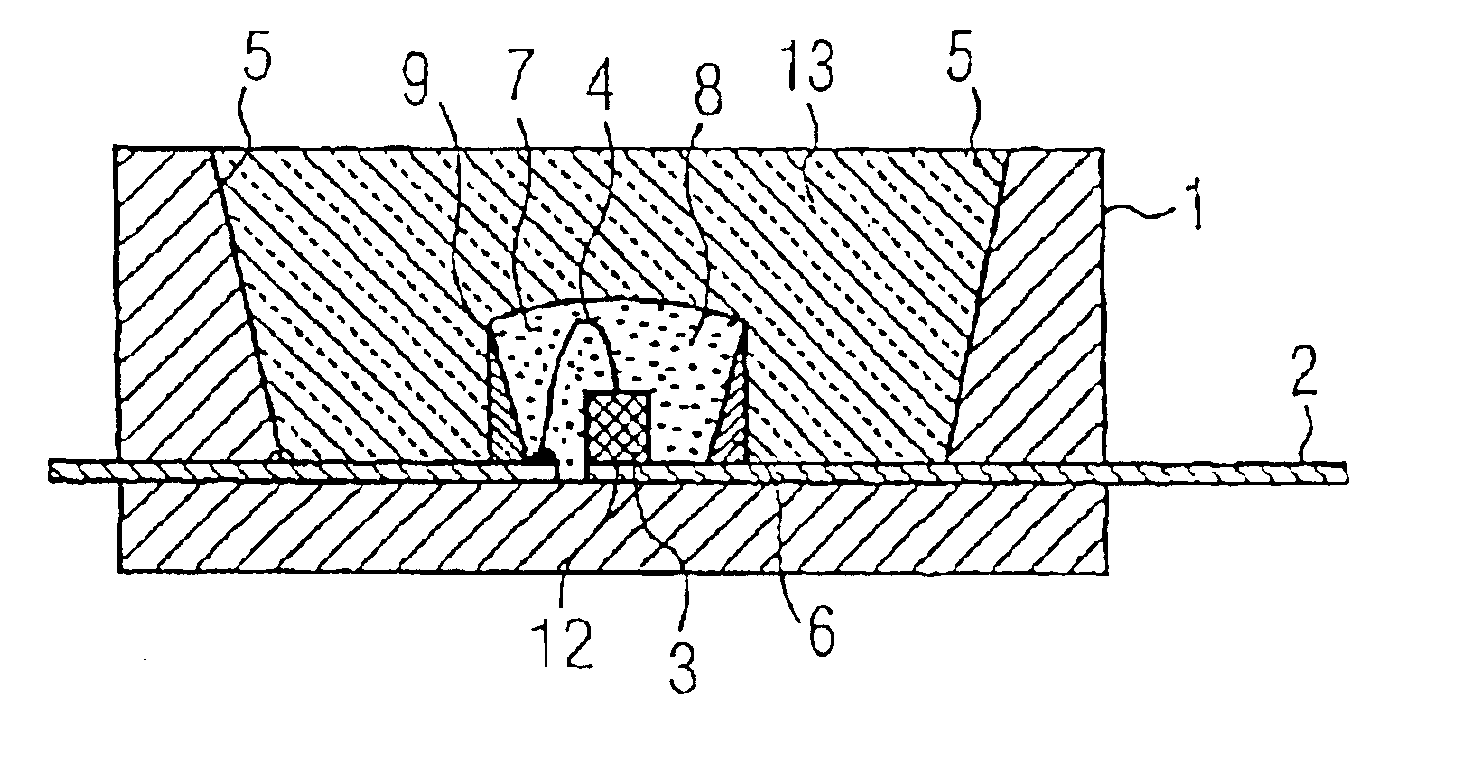
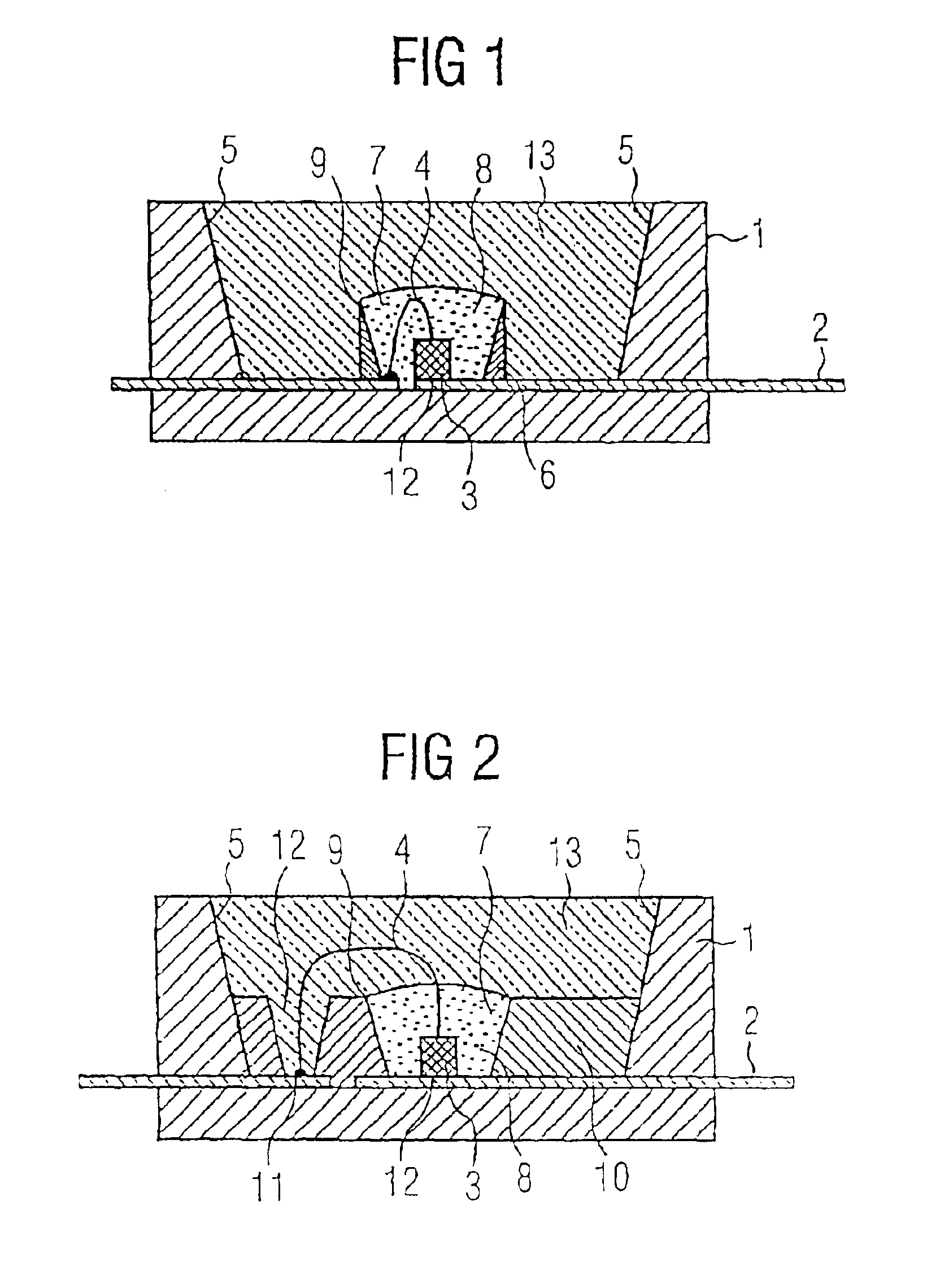
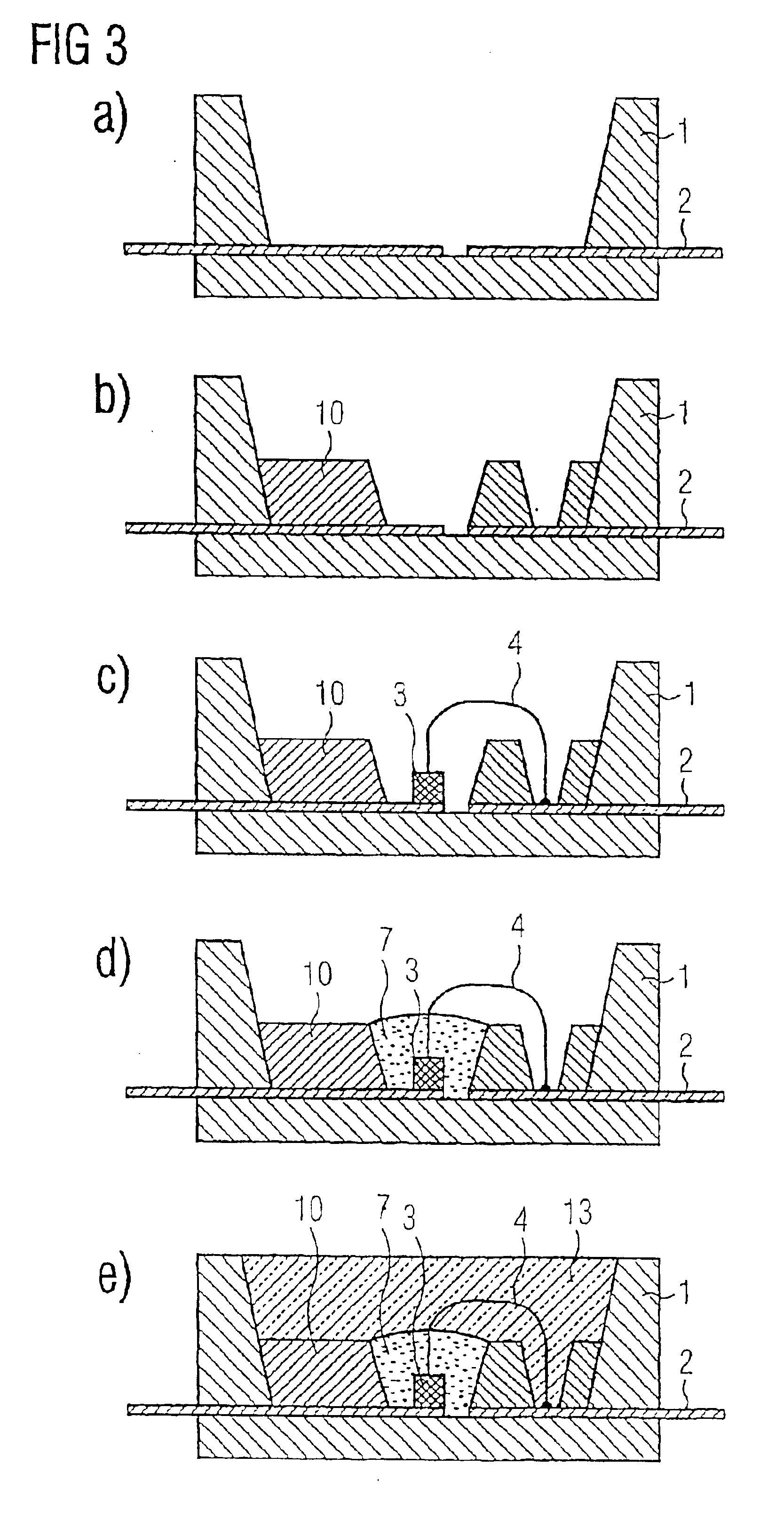
[0034]In the following disclosure, like numerals refer to like elements. The semiconductor component shown in FIG. 1, according to the invention, is a standard casing body material 1. The body may be a unibody made from a single piece of material. This can for example be an LED-casing installed on the surface which comprises thermoplast. The body or base body includes an interior recess, open internal region or groove defined by side walls 5. The side walls 5 are slightly slanted and act as a reflector for radiation produced there between. A conductor frame 2 is integrated into the body material 1, running within the base body so as to define a floor for the open internal region and specific areas described below. A semiconductor body 3 is bonded a the chip service area 12 located atop conductor frame 2. The semiconductor body is electrically connected by a wire connection 4 with the wire service area 11 of the conductor frame 2. The bonding of the semiconductor body 3 can occur as ...


PUM


Abstract

The invention describes a radiation-emitting semiconductor component with a luminescent conversion element, at which the semiconductor body is placed in a recess of the base body. A cup-like area is molded inside of the recess around the semiconductor body, which contains the luminescent conversion element and coats the semiconductor body. The cup-like portion is formed as indentation inside of the recess or as annular border on the base of the recess.

Description

CROSS REFERENCE TO RELATED APPLICATIONS[0001]The present application is a continuation of International Application No. PCT / DE01 / 01601, filed 26 Apr. 2001 which designated the United States, and claims priority to German patent application no. DE10020465.1, filed 26, Apr. 2000 both of which are incorporated herein by reference.STATEMENT REGARDING FEDERALLY SPONSORED RESEARCH OR DEVELOPMENT[0002]Not Applicable.REFERENCE TO SEQUENCE LISTING, A TABLE, OR A COMPUTER PROGRAM LISTING COMPACT DISK APPENDIX[0003]Not Applicable.BACKGROUND OF THE INVENTION[0004]The invention generally relates to a radiation emitting semiconductor component and more particularly to a semiconductor component and method of making the same wherein the component demonstrates improved radiated multi-colored light homogeneity.[0005]An example of light emitting semiconductor components is set out in WO 97 / 50132 Such components contain a semiconductor body which emits light (primary light) and a luminescent conversion...

Claims


Application Information

Patent Timeline
Patent Type & Authority Patents(United States)
IPC IPC(8): H01L33/00H01L33/48H01L33/50H01L33/60H01L33/62
CPCH01L33/486H01L33/505H01L33/60H01L33/62H01L2933/0041H01L2224/48247H01L2224/48091H01L2924/12041H01L2224/48471H01L2924/00014H01L2924/181H01L2224/8592H01L2924/00012H01L2224/4554
Inventor BRUNNER, HERBERTDEBRAY, ALEXANDRAJĀGER, HARALDWAITL, GUNTHER
Owner OSRAM GMBH
Why Eureka
Try Eureka