System and method for product yield prediction

a technology of product yield prediction and system, applied in the direction of computer control, semiconductor/solid-state device testing/measurement, instruments, etc., can solve the problems of defective integrated circuits, circuit defects, and extremely complex process of integrated circuit fabrication

Inactive Publication Date: 2005-05-31
PDF SOLUTIONS INC
View PDF40 Cites 142 Cited by
  • Summary
  • Abstract
  • Description
  • Claims
  • Application Information

AI Technical Summary

Problems solved by technology

The fabrication of integrated circuits is an extremely complex process that may involve hundreds of individual operations.
For example, in the photoresist and photomask operations, the presence of contaminants such as dust, minute scratches and other imperfections in the patterns on the photomasks can produce defective patterns on the semiconductor wafers, resulting in defective integrated circuits.
Further, defects can be introduced in the circuits during the diffusion operations themselves.
In the past, many of the defects which caused poor yield in integrated circuits were caused by particulate contaminants or other random sources.
Examples of these systematic defect sources include printability problems from using aggressive lithography tools, poly stringers from poorly formed silicides, gate length variation from density driven and optical proximity effects.
In attempting to decrease the number of defective integrated circuits produced in the manufacturing process, thus increasing the yield, one is faced with the fact that any one or more of possibly several hundred processing steps may have caused a particular circuit to be defective.
With such a large number of variables to work with, it can be extremely difficult to determine the exact cause or causes of the defect or defects in a particular circuit thereby making it extraordinarily difficult to identify and correct the yield detracting process operations.
However, inspection equipment often does not capture many of the systematic defect sources and / or the tools can be difficult to tune, optimize, or use effectively and reliably.
Furthermore, inspection equipment, especially in recent technologies is often plagued with many false alarms or nuisance defects, as they are known, which serve to frustrate any attempts to reliably observe true defects or sources of defects.
It is typically discovered that, once a particular problem has been identified at final test after completion of the fabrication cycle, it can be confirmed that a problem in a particular process operation did exist at the time that operation was carried out, which could have been weeks or even months earlier.
At this time, different process operations may be causing problems.
Thus, after the fact analysis of defective integrated circuits and identification of process operations causing these defective products is severely limited as a means for improving the overall yield of integrated circuits.

Method used


Image

  • System and method for product yield prediction
  • System and method for product yield prediction
  • System and method for product yield prediction

Examples


Embodiment Construction

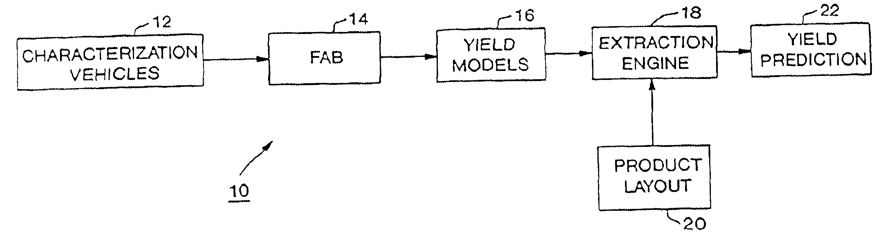
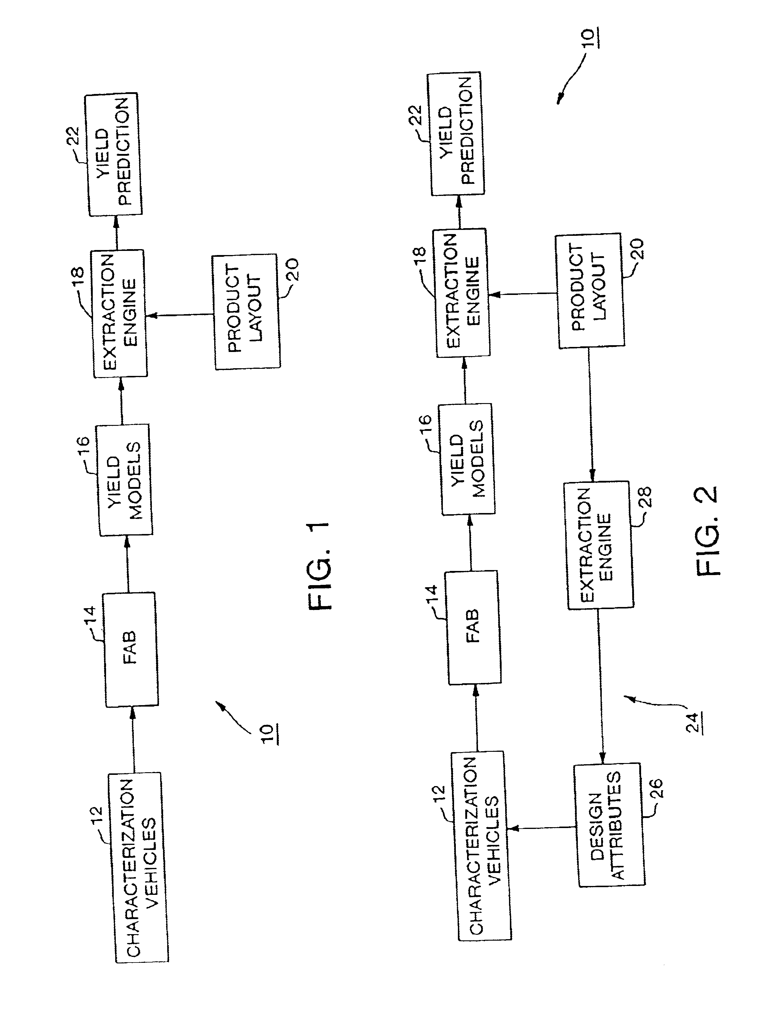
[0032]Referring now to FIG. 1, there is shown a block diagram depicting the steps performed by a system, generally designated 10, for predicting integrated circuit yields in accordance with the present invention. The system 10 utilizes at least one type of characterization vehicle 12. The characterization vehicle 12 preferably is in the form of software containing information required to build an integrated circuit structure which incorporates at least one specific feature representative of at least one type of feature to be incorporated into the final product. For example, the characterization vehicle 12 might define a short flow test vehicle of a single lithographic layer for probing the health and manufacturability of the metal interconnection module of the process flow under consideration. The structures need to be large enough and similar enough to the actual product or type of products running in the fabrication-process to enable a reliable capture or fingerprint of the variou...


PUM


Abstract

A yield for an integrated circuit is predicted by processing a wafer to have a portion fabricated with at least one layout attribute of the integrated circuit. The portion of the wafer is analyzed to determine an actual yield associated with the at least one layout attribute. A systematic yield associated with the at least one layout attribute is determined based on the actual yield and a predicted yield associated with the at least one layout attribute. The predicted yield assumes that random defects are the only yield loss mechanism. A yield of an actual or proprosed product layout is predicted for the integrated circuit based on the systematic yield.

Description

CROSS-REFERENCE TO RELATED APPLICATION[0001]This application is a continuation application of U.S. patent application Ser. No. 09 / 442,699, entitled SYSTEM AND METHOD FOR PRODUCT YIELD PREDICTION, filed on Nov. 18, 1999, which has issued as U.S. Pat. No. 6,449,749, issued on Sep. 10, 2002.BACKGROUND OF THE INVENTION[0002]The present invention pertains to fabrication of integrated circuits and more particularly to systems and methods for improving fabrication yields.[0003]The fabrication of integrated circuits is an extremely complex process that may involve hundreds of individual operations. Basically, the process includes the diffusion of precisely predetermined amounts of dopant material into precisely predetermined areas of a silicon wafer to produce active devices such as transistors. This is typically done by forming a layer of silicon dioxide on the wafer, then utilizing a photomask and photoresist to define a pattern of areas into which diffusion is to occur through a silicon ...

Claims


Application Information

Patent Timeline
Patent Type & Authority Patents(United States)
IPC IPC(8): H01L21/66H01L23/544H01L21/00G01R31/26G05B15/02H01L21/02
CPCG05B15/02G06F17/5081H01L22/20H01L22/34H01L2924/0002H01L2924/00G06F30/398
Inventor STINE, BRIAN E.HESS, CHRISTOPHERKIBARIAN, JOHNMICHAELS, KIMONDAVIS, JOSEPH C.MOZUMDER, PURNENDU K.LEE, SHERRY F.WEILAND, LARG H.CIPLICKAS, DENNIS J.STASHOWER, DAVID M.
Owner PDF SOLUTIONS INC
Why Eureka
Try Eureka