Semiconductor component having backside pin contacts

a technology of backside pin contacts and semiconductors, applied in the direction of semiconductor devices, semiconductor/solid-state device details, electrical devices, etc., can solve the problems of affecting the reliability of components, requiring relatively complicated interconnections, and prior art components

Inactive Publication Date: 2005-06-07
MICRON TECH INC
View PDF43 Cites 167 Cited by
  • Summary
  • Abstract
  • Description
  • Claims
  • Application Information

AI Technical Summary

Problems solved by technology

Some prior art components require relatively complicated interconnections, such as metal beams or wires, formed of gold, gold plated materials, aluminum, copper or solder using a bonding process, such as thermosonic bonding or wire bonding.
These stresses can cause the interconnections to weaken or pull apart, adversely affecting the reliability of the components.

Method used


Image

  • Semiconductor component having backside pin contacts
  • Semiconductor component having backside pin contacts
  • Semiconductor component having backside pin contacts

Examples


Embodiment Construction

[0032]As used herein, the term “semiconductor component” refers to an electronic element that includes a semiconductor die. Exemplary semiconductor components include semiconductor packages, chip scale packages, semiconductor dice, BGA devices, and semiconductor wafers.

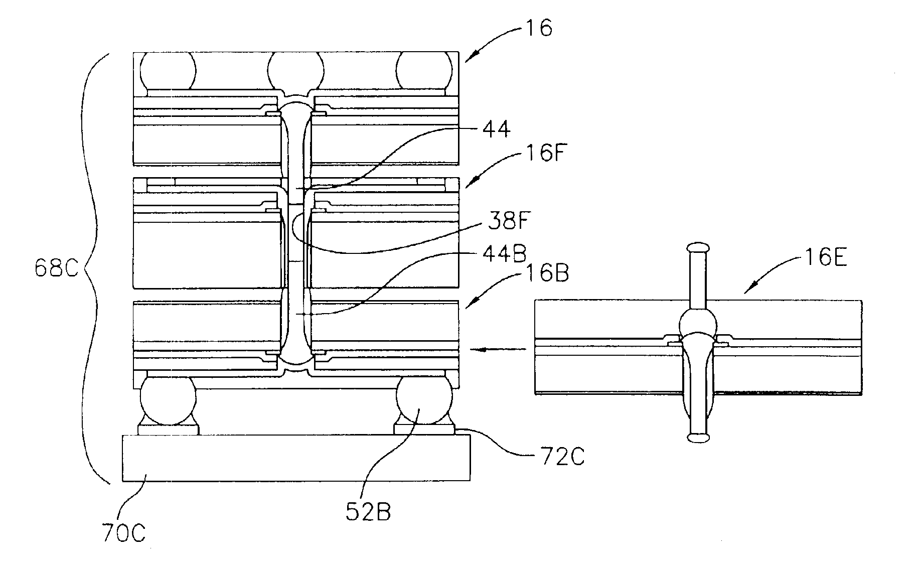
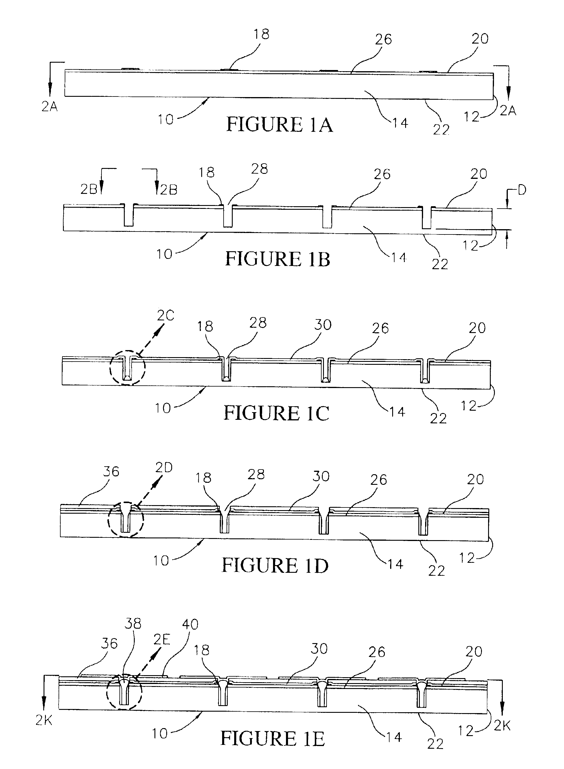
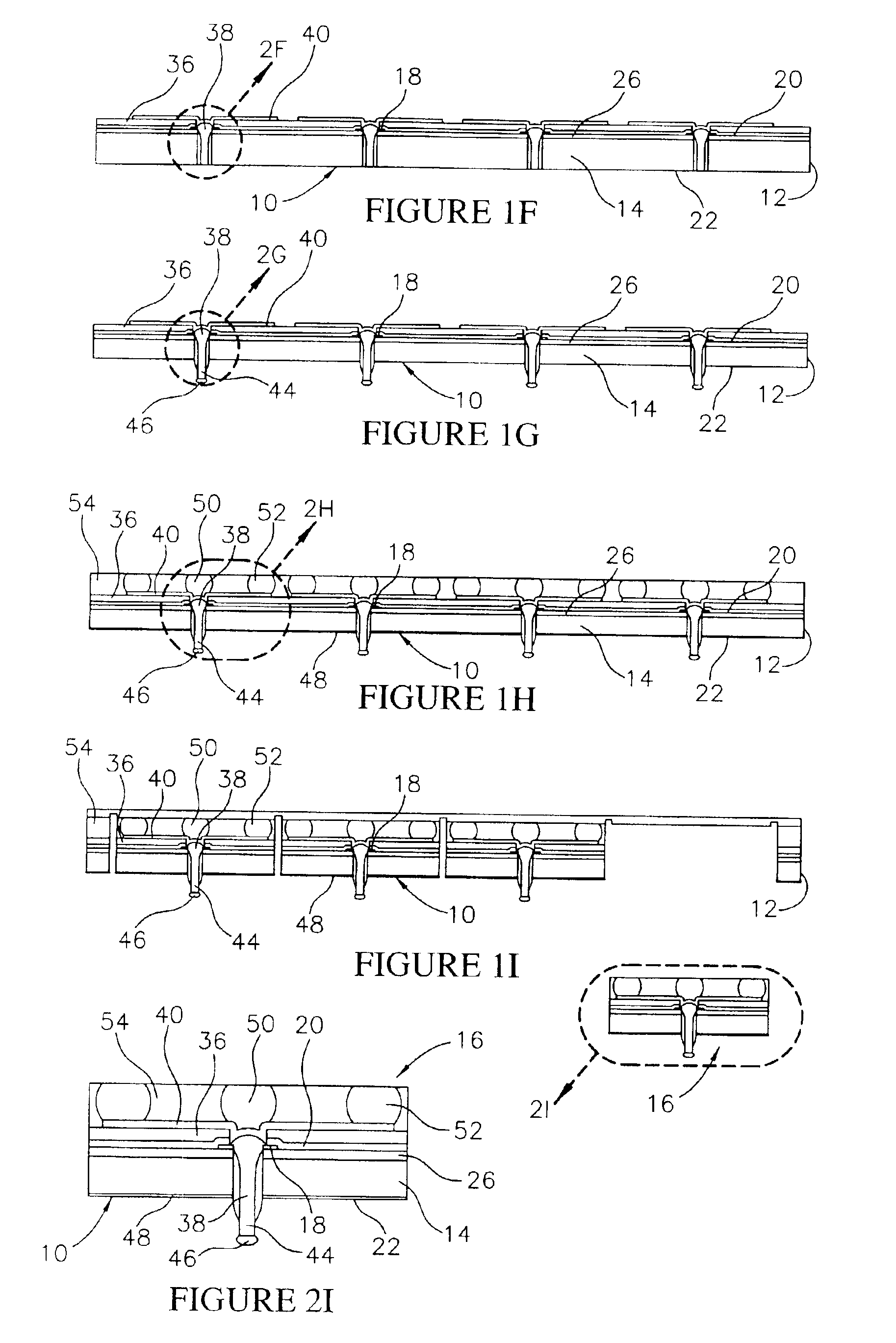
[0033]Referring to FIGS. 1A-1I and 2A-2K, steps in the method for fabricating a semiconductor component 16 (FIG. 2I) in accordance with the invention are illustrated.

[0034]Initially, as shown in FIGS. 1A and 2A, a plurality of semiconductor dice 10 are provided, for fabricating a plurality of semiconductor components 16 (FIG. 2I).

[0035]The dice 10 can comprise conventional semiconductor dice having a desired configuration. For example, each die 10 can comprise a dynamic random access memory (DRAM), a static random access memory (SRAM), a flash memory, a microprocessor, a digital signal processor (DSP) or an application specific integrated circuit (ASIC). The dice 10 and the components 16 can have any polygonal shape. ...


PUM


Abstract

A semiconductor component includes back side pin contacts fabricated using a circuit side fabrication method. The component also includes a thinned semiconductor die having a pattern of die contacts, and conductive members formed by filled openings in the die contacts and the die. In addition, the pin contacts are formed by terminal portions of the conductive members. The fabrication method includes the steps of forming the openings and the conductive members, and then thinning and etching the die to form the pin contacts. An alternate embodiment female component includes female conductive members configured to physically and electrically engage pin contacts on a mating component of a stacked assembly.

Description

FIELD OF THE INVENTION[0001]This invention relates generally to semiconductor manufacture and packaging. More particularly, this invention relates to a semiconductor component with backside contacts, to a method for fabricating the component, and to systems incorporating the component.BACKGROUND OF THE INVENTION[0002]Semiconductor components, such as chip scale packages and bumped dice, are being manufactured with a smaller outline and with a higher pin count than conventional plastic or ceramic packages. This type of semiconductor component typically includes a dense area array of terminal contacts, such as solder bumps in a ball grid array (BGA) or metal pins in a pin grid array (PGA). The terminal contacts permit the component to be surface mounted to a supporting substrate, such as a package substrate, a module substrate or a circuit board.[0003]The quality, reliability and cost of these types of components is often dependent on the fabrication method. The formation of the termi...

Claims


Application Information

Patent Timeline
Patent Type & Authority Patents(United States)
IPC IPC(8): H01L25/065H01L23/48
CPCH01L21/76831H01L21/76898H01L23/3114H01L23/481H01L24/11H01L25/0657H01L25/50H01L24/13H01L2924/0001H01L2224/131Y10S438/977H01L2224/13099H01L2224/16H01L2225/06541H01L2225/06586H01L2924/01005H01L2924/01013H01L2924/01022H01L2924/01029H01L2924/0103H01L2924/01042H01L2924/01046H01L2924/01047H01L2924/01073H01L2924/01074H01L2924/01075H01L2924/01077H01L2924/01078H01L2924/01079H01L2924/14H01L2924/1433H01L2924/01006H01L2924/01019H01L2924/01024H01L2924/01033H01L2924/01072H01L2924/014H01L24/03H01L24/05H01L2224/05001H01L2224/05009H01L2224/05172H01L2224/0557H01L2224/05572H01L2224/1134H01L2924/12042H01L2924/00H01L2924/00014H01L2224/05624H01L2224/05639H01L2224/05644H01L2224/05655H01L2224/05666H01L2224/05671H01L2224/05681H01L2224/05684H01L2224/05111H01L2224/05124H01L2224/05139H01L2224/05144H01L2224/05147H01L2224/05155H01L2224/05164H01L2224/05166H01L2224/05169H01L2224/05184
Inventor WOOD, ALAN G.DOAN, TRUNG TRI
Owner MICRON TECH INC
Why Eureka
Try Eureka