Liquid crystal screen display

a liquid crystal screen and display technology, applied in optics, thin material processing, instruments, etc., can solve the problems of ips mode liquid crystal screen display array substrates, unable to meet the needs of liquid crystal screen display, and the display is most likely to be uneven, so as to achieve the effect of limiting display unevenness

Inactive Publication Date: 2005-06-14
BISHOP DISPLAY TECH LLC
View PDF15 Cites 6 Cited by
  • Summary
  • Abstract
  • Description
  • Claims
  • Application Information

AI Technical Summary

Benefits of technology

[0013]A primary object of the invention is to provide a liquid crystal screen display capable of restraining display unevenness attributable to ions which have been locally generated within the liquid crystal layer and displaying satisfactory images for a long time.
[0018]Occurrence of electrical short can be more effectively restrained by forming an insulating film on the surfaces of the gate signal lines by anodic oxidation in the regions where the gate signal lines intersect other signal lines. For instance, the regions above which an aperture is to be formed and the regions (e.g., connector terminals) where the conductivity of the surfaces of signal lines needs to be ensured are masked while an anodic oxidation film being selectively formed in other regions. As the material of the gate signal lines, aluminum, tantalum, zirconium and alloys containing these metals in an amount of 80 wt % or more are suitably used in the light of easy anodic oxidation and the stability of an oxide film to be formed.
[0022]When forming the lower electrodes and the gate signal lines at the same time, a sufficient margin can be obtained between the gate signal lines and the electrodes formed on the same layer as the gate signal lines by providing electrode components for a region adjacent the gate signal lines. In this way, occurrence of electrical short at the time of formation of these elements can be restrained. Electrode components are positioned in the vicinity of the gate signal lines but formed on a layer different from the layer on which the gate signal lines are formed, with an insulating layer being interposed between these layers.
[0023]In addition, the signal lines or the electrodes on the upper layer can be easily exposed by providing an overcoat film for only the region including a switching element while no overcoat film is laid over the electrodes and the signal lines.
[0027]Provision of a conductive member for ion generation for every pixel most effectively restrains occurrence of display unevenness. It is apparent that a conductive member may be provided for every specified number of pixels. The distribution of the conductive members is determined taking into consideration their ion generation capability as well as the influence of their arrangement upon the display quality of the panel. The distribution of the conductive members for ion retrieval is also determined by taking account of their ion retrievablility and the influence of their arrangement upon the display quality of the panel. Since the visibility of humans to luminance variations in blue is lower than to luminance variations in other colors (i.e., red and green), provision of the conductive members for blue pixels reduces a feeling of physical disorder given to human beings, compared to the case where other color pixels are provided with the conductive members.
[0028]In another liquid crystal screen display of the invention, electrolytic salt is added for forming ions within the liquid crystal layer. Where electrolytic salt is added to the liquid crystal layer beforehand, even if ions are locally generated, the difference in ion concentration between regions and, in consequence, display unevenness occurring in the panel are reduced.

Problems solved by technology

The TN mode liquid crystal screen displays do not have a sufficiently wide angle of view.
In the formation of electrodes and signal lines on a substrate for liquid crystal screen displays, these elements are liable to electrical short owing to contamination with dust particles or pattern defects of the electrodes.
Above all, array substrates for IPS mode liquid crystal screen displays are most likely to cause electrical short in their formation process because of the provision of comb-like pixel electrodes and common electrodes.
If the short-circuited portions are isolated by laser irradiation, the portions of the overcoat film which have been irradiated with the laser beams tend to be destroyed so that the signal lines and others reveal from the overcoat film.
If the gate signal lines are exposed resulting from the laser irradiation, display unevenness is likely to occur in the regions repaired by the laser irradiation, when the liquid crystal screen display having such a substrate is continuously driven.
The local uneven distribution of ions causes a drop in the voltage retention of the liquid crystal layer of these regions and, in consequence, display unevenness.
Similar display unevenness occurs, for example, in cases where pin holes are created in the overcoat film laid over the gate signal lines or where the gate signal lines have level differences.
According to this publication, although the exposure of the electrodes to the liquid crystal layer through pin holes can be reduced by use of an overcoat film having sufficient thickness, it has no effect of restraining the exposure of signal lines and others due to the destruction of the overcoat film by laser irradiation.
However, since the voltage of the pixel electrodes is retained only by the storage capacitor during most of the period of time when the panel is driven, active retrieval of ions results in a drop in interelectrode voltage.
More concretely, the ion concentration of the liquid crystal layer cannot be effectively reduced.
Selection of a liquid crystal material based on resistivity is not necessarily appropriate in view of prevention of image persistence and high-speed response.

Method used


Image

  • Liquid crystal screen display
  • Liquid crystal screen display
  • Liquid crystal screen display

Examples


first embodiment

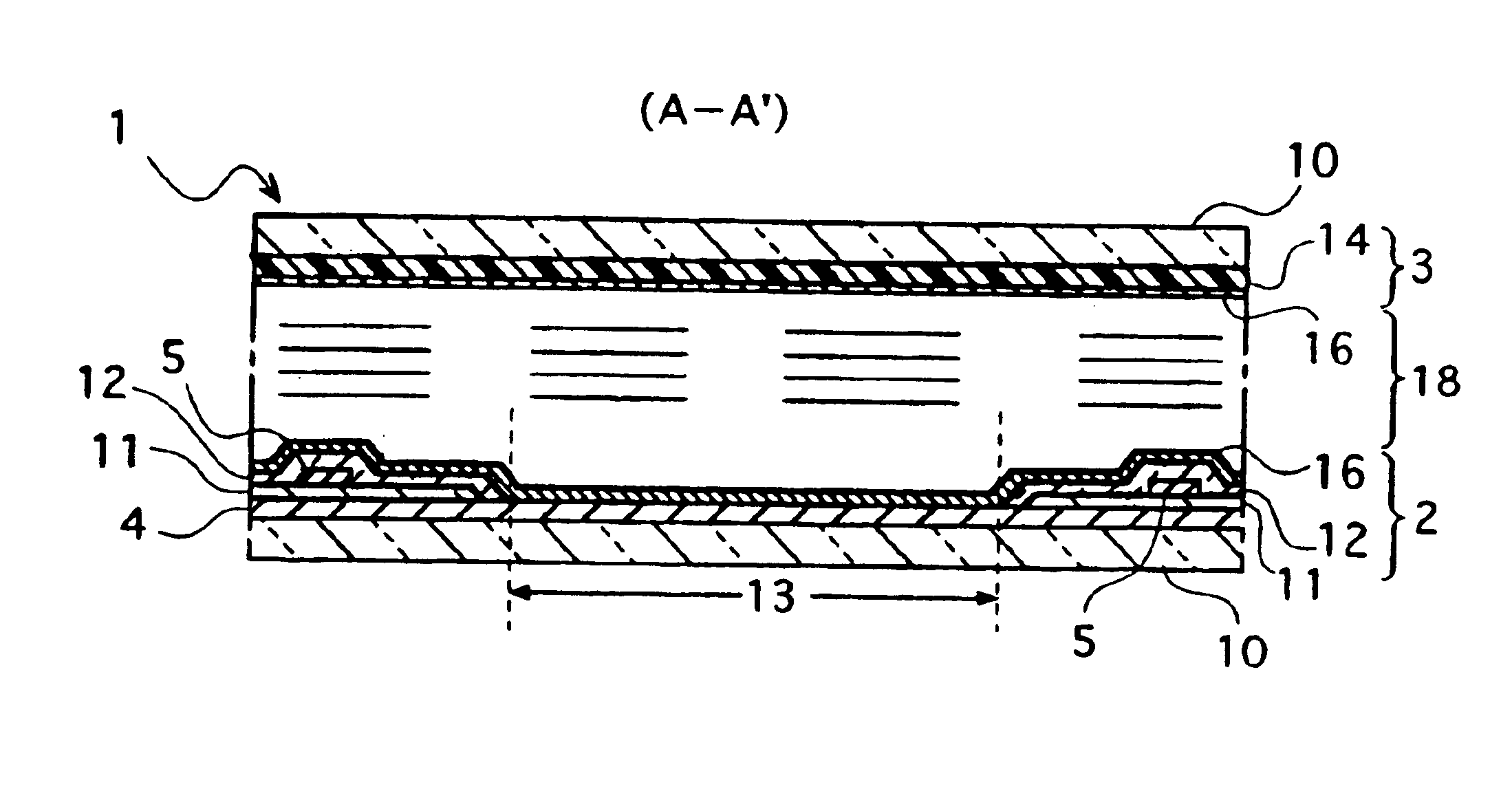
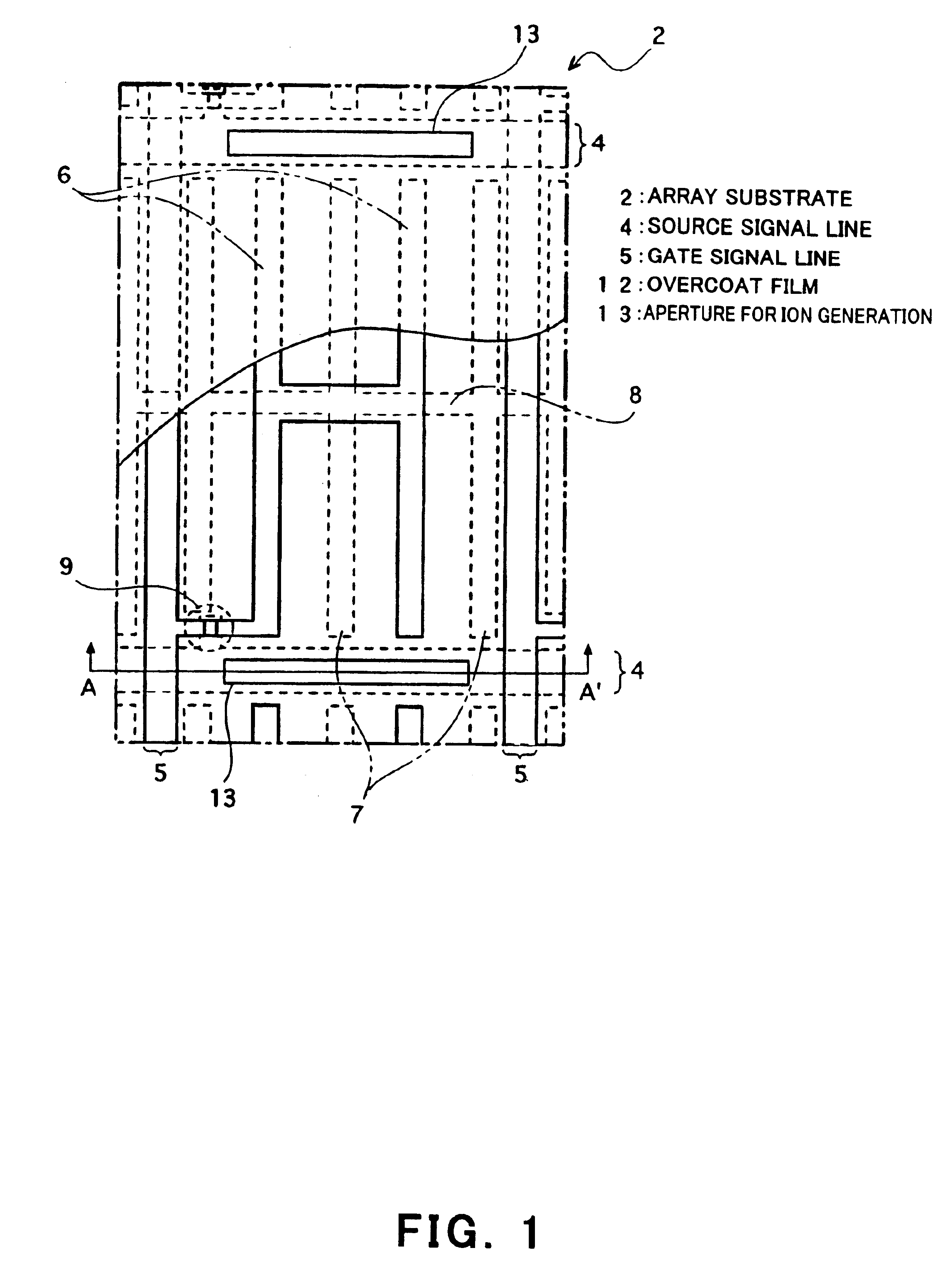
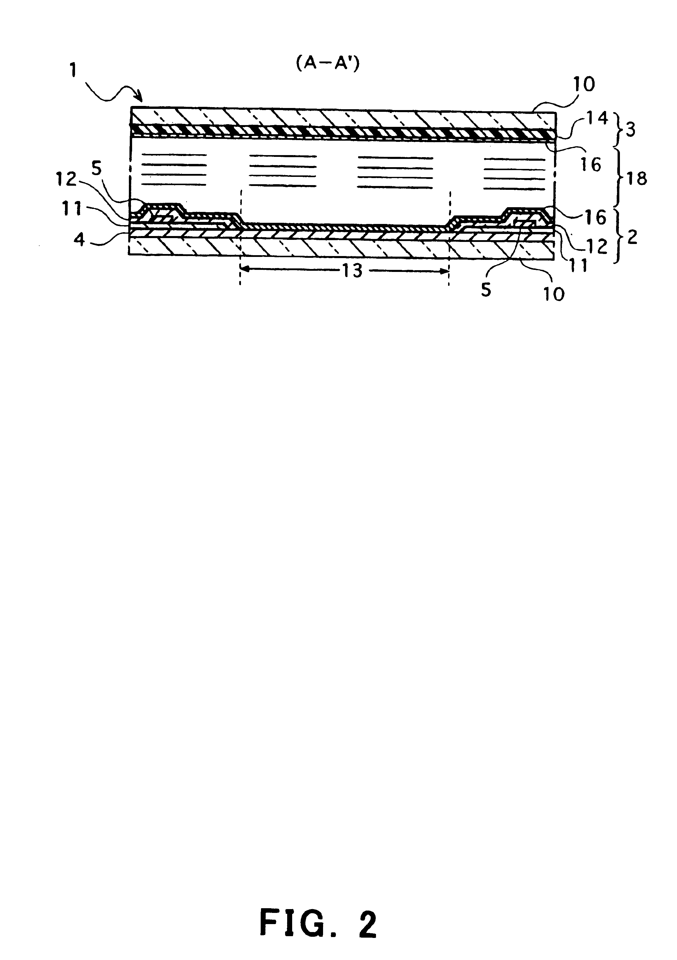
[0050]FIG. 1 shows an array substrate for use in a liquid crystal screen display of the first embodiment. The liquid crystal screen display employing this array substrate is shown in FIG. 2.

[0051]The array substrate 2 has electrodes and signal lines in a similar layout to that of the array substrate of the prior art shown in FIG. 17. In a pixel region enclosed by a pair of gate signal lines 4 and a pair of source signal lines 5, pixel electrodes 6 and common electrodes 7, which are both comb-like in shape, are placed with an insulating layer 11 between. The common electrodes 7 in one pixel region are electrically connected to common electrodes 7 within the right and left adjacent pixel regions shown in FIG. 1 through a common electrode line 8 that is integrally formed with the common electrodes 7. The source signal lines 5 formed on the same layer as the pixel electrodes 6 are connected to the pixel electrodes 6 through a thin film transistor (TFT) 9. The gate signal lines 4 are for...

second embodiment

[0069]While the first embodiment has been presented in terms of gate signal lines used as a member for ion generation, the second embodiment is associated with another form.

[0070]A third electrode, which is formed in contact with the alignment layer independently of the pixel electrodes and the common electrodes, is provided for the conventional liquid crystal screen display as a conductive member for ion generation, whereby a liquid crystal screen display capable of restraining occurrence of display unevenness due to uneven ion distribution can be obtained, similarly to the first embodiment. The liquid crystal screen display according to the second embodiment comprises the array substrate 2 having a structure similar to that of the conventional liquid crystal screen display shown in FIG. 17 and the opposed substrate 3 which includes a third electrode 17 having a negative potential with respect to the electrodes 6 and 7, as shown in FIG. 5.

[0071]The third electrode 17 is in contact ...

third embodiment

[0073]If ions are continuously generated like the foregoing embodiments, the resistivity of the liquid crystal layer gradually decreases, restraining display unevenness, while there is the possibility of deterioration in display quality due to a constant decline in voltage retention during long use. Although it is possible to compensate for such changes by use of drive signals, the third embodiment will be described in terms of one example of liquid crystal screen displays capable of fundamentally preventing deterioration in display quality without compensation by use of such drive signals.

[0074]FIG. 6 shows an array substrate for use in the liquid crystal screen display of the third embodiment. FIGS. 7a and 7b show the liquid crystal screen display of the third embodiment.

[0075]The liquid crystal screen display of the third embodiment has apertures 13a for ion generation and an aperture 13b for ion retrieval. The apertures 13a are formed in parts of the gate signal lines by removin...


PUM

PropertyMeasurementUnit
temperatureaaaaaaaaaa
side lengthaaaaaaaaaa

Abstract

A liquid crystal screen display is disclosed which is capable of restraining occurrence of display unevenness. In the display of the invention, a conductive member to which a negative voltage is applied is placed between a substrate and an alignment layer so as to be in partial contact with the alignment layer. Uneven ion distribution attributable to ion generation within broken or pin hole parts of an overcoat film is restrained, for instance, by exposing gate signal lines etc. to the alignment layer so that ions are intentionally generated in the regions of the liquid crystal layer corresponding to the exposed regions.

Description

TECHNICAL FIELD[0001]The present invention relates to a liquid crystal screen display and more particularly to an improved method for restraining occurrence of display unevenness in active matrix liquid crystal screen displays.BACKGROUND ART[0002]Liquid crystal screen displays possess advantages such as thinness, light weight, and applicability to low-voltage driving, and therefore, they have been used in many display applications including wrist watches, desk-top calculators, personal computers and word processors as well as in light shutter applications.[0003]The most popular liquid crystal screen displays are the Twisted Nematic (TN) mode liquid crystal screen displays in which a liquid crystal layer is held between a pair of substrates and electrodes are placed on the respective substrates, for establishing an electric field for driving liquid crystal molecules in the liquid crystal layer. The TN mode liquid crystal screen displays do not have a sufficiently wide angle of view. ...

Claims


Application Information

Patent Timeline
Patent Type & Authority Patents(United States)
IPC IPC(8): G02F1/1337G02F1/13G02F1/1362G02F1/1345G02F1/1343
CPCG02F1/1337G02F1/1345G02F1/136286G02F1/134363Y10T428/1036G02F2001/133796Y10T428/10C09K2323/00C09K2323/03G02F1/133796G02F1/1343
Inventor SATO, ICHIROKUMAGAWA, KATSUHIKOINOUE, KAZUONISHIYAMA, KAZUHIRO
Owner BISHOP DISPLAY TECH LLC
Why Eureka
Try Eureka