Method and apparatus for probe tip cleaning and shaping pad

Inactive Publication Date: 2005-06-21
SV PROBE PTE LTD
View PDF19 Cites 71 Cited by
  • Summary
  • Abstract
  • Description
  • Claims
  • Application Information

AI Technical Summary

Problems solved by technology

In particular, due to the time and expense required to package a semiconductor chip, and given the probability that a particular semiconductor chip may have a flaw, it is common practice to inspect the wafers before the wafers are cut up into individual chips.
If a poor electrical connection is made between the probe device and the electrodes, an incorrect status for a chip may be obtained.
A blunt probe tip may make the probe tip less effective at scratching the surface of the electrode.
A blunted probe tip may also cause probe marks to go beyond the specified allowable electrode contact area on the wafer if the blunt end of the tip becomes too large.
A further problem related to the blunting of a probe tip, is that uneven blunting of probe tips creates probes of different lengths which may cause planarity problems.
Probes may wear unevenly because sometimes some of the probes may be probing portions of the wafer where no electrodes exist and the probes touch down on materials of different hardness than the elec

Method used


Image

  • Method and apparatus for probe tip cleaning and shaping pad
  • Method and apparatus for probe tip cleaning and shaping pad
  • Method and apparatus for probe tip cleaning and shaping pad

Examples


Embodiment Construction

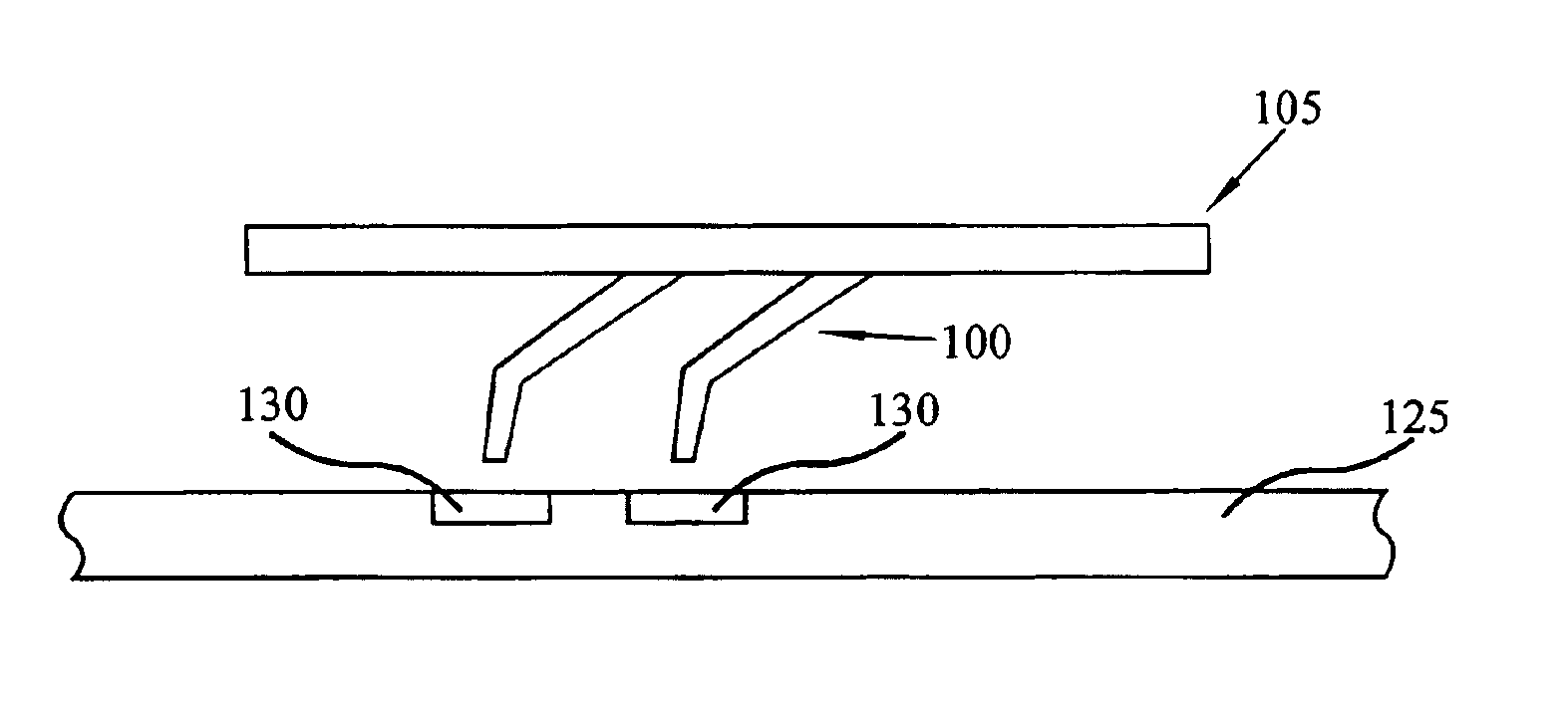
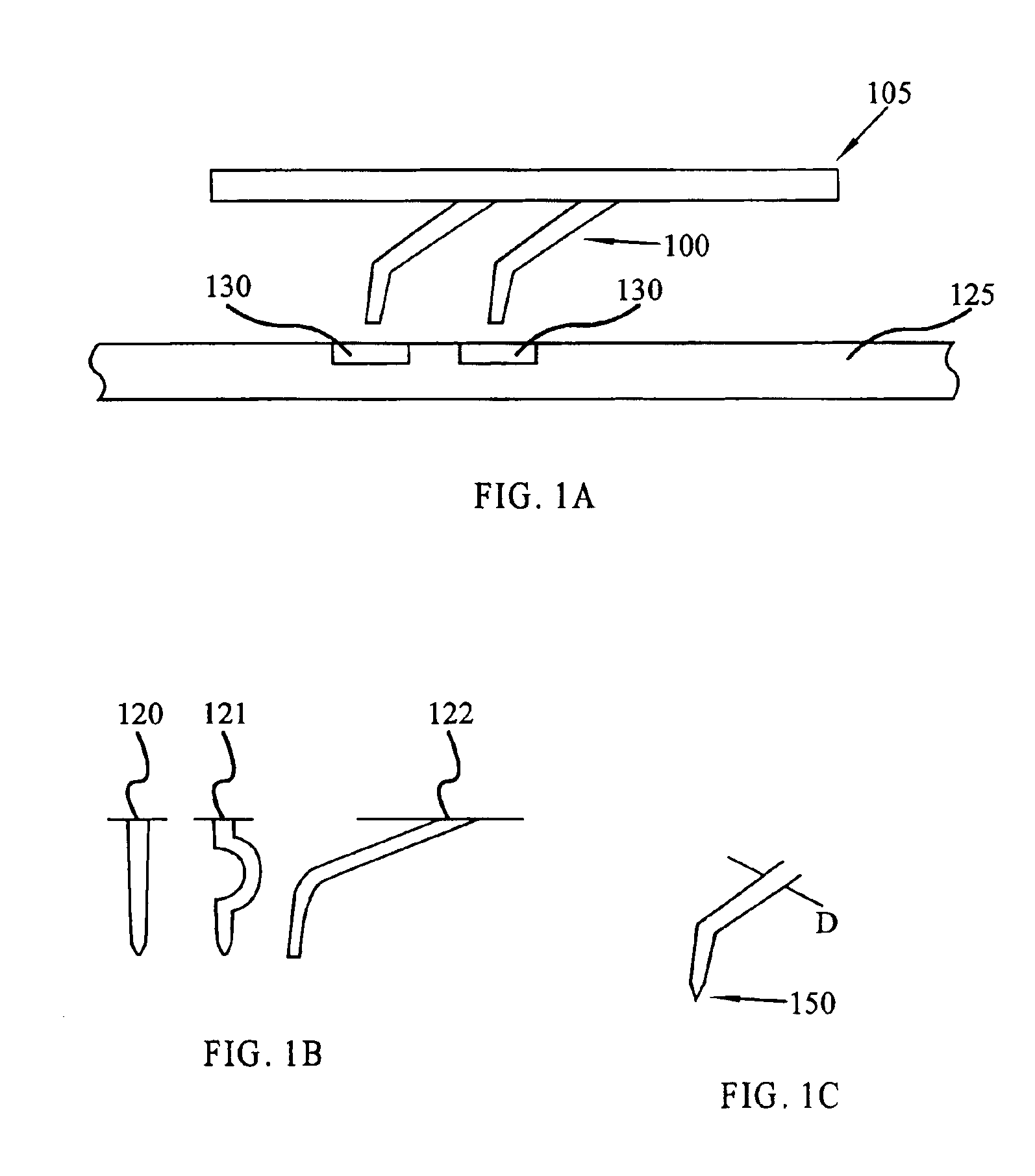
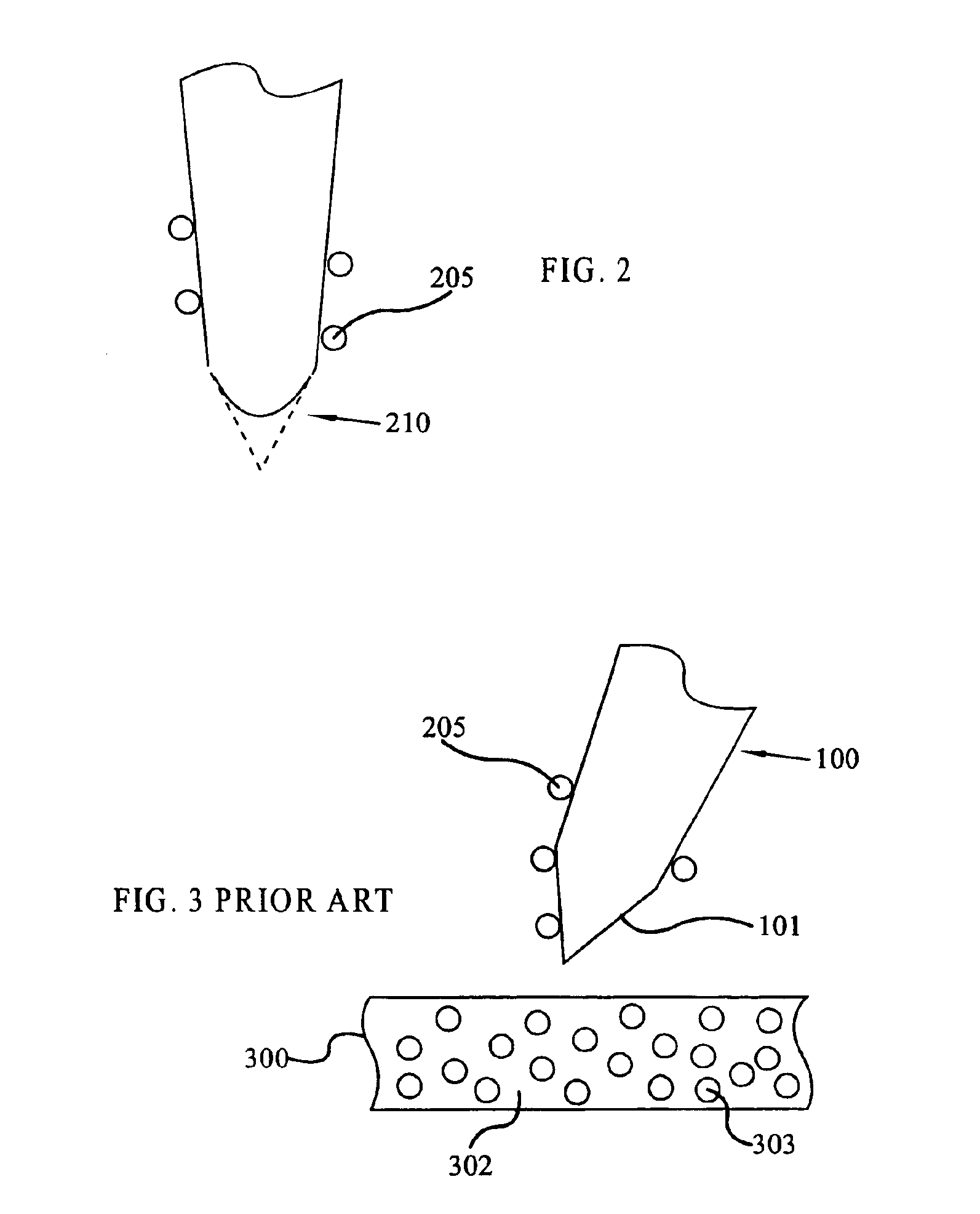
[0021]The present invention may be described herein in terms of various hardware components and processing steps. It should be appreciated that such components may be realized by any number of hardware components configured to perform the specified functions. For example, the present invention may employ various integrated circuit components, e.g., transistors, memory elements, digital signal processing elements, integrators, motors, actuators, servos, gears, and the like, which may carry out a variety of functions under the control of one or more microprocessors or other control devices. Moreover, various types of material may be used in making the probe tip cleaning and shaping pads. In addition, those skilled in the art will appreciate that the present invention may be practiced in any number of probing device contexts and that the preferred embodiment described herein is merely one exemplary application for the invention. General techniques that may be known to those skilled in ...


PUM

PropertyMeasurementUnit
Thicknessaaaaaaaaaa
Lengthaaaaaaaaaa
Sizeaaaaaaaaaa

Abstract

A method and apparatus is provided for cleaning and shaping a probe tip using a multi-layer adhesive and abrasive pad. The multi-layer adhesive and abrasive pad is constructed on the surface of a support structure, such as a silicon wafer, and is made of an adhesive in contact with abrasive particles. Adhesive is applied in layers with abrasive particles in-between each layer of adhesive. Abrasive particles may vary in size and material from layer to layer to achieve cleaning, shaping and polishing objectives.

Description

FIELD OF INVENTION[0001]The present invention relates to a cleaning and shaping pad, and to a probe tip cleaning and shaping pad.BACKGROUND OF THE INVENTION[0002]In the field of semiconductor manufacturing, it is common practice to test the semiconductor chips at various stages in the manufacturing process. In particular, due to the time and expense required to package a semiconductor chip, and given the probability that a particular semiconductor chip may have a flaw, it is common practice to inspect the wafers before the wafers are cut up into individual chips. To facilitate this testing, small conductive pads (electrodes) are often located on the surface of the wafer that may be used to connect chip circuitry to an external tester such as a probe device. The probe device may send electrical signals through these electrodes to the circuitry on the wafer. The probe device may also receive electrical response signals from the wafer through these electrodes. These response signals ca...

Claims


Application Information

Patent Timeline
IPC IPC(8): B24D3/20B24D18/00B24D3/28B24B19/16B24B29/00B24B29/08B24B19/00B24D13/00B24D13/14
CPCB24B19/16B24B29/08B24D18/0072B24D13/142B24D18/0045B24D3/28
Inventor BACK, GERALD W.DANG, SONTUNABOYLU, BAHADIR
Owner SV PROBE PTE LTD
Why Eureka
Try Eureka