Mounting structure of dielectric filter, dielectric filter device, mounting structure of dielectric duplexer, and communication device

a technology of mounting structure and dielectric filter, which is applied in the direction of resonators, electrical equipment, waveguides, etc., can solve the problem of not being able to obtain the best characteristics of the tem mode to be used, and achieve the effect of excellent communication characteristics

Inactive Publication Date: 2005-06-21
MURATA MFG CO LTD
View PDF2 Cites 33 Cited by
  • Summary
  • Abstract
  • Description
  • Claims
  • Application Information

AI Technical Summary

Benefits of technology

[0021]A communication device of the present invention comprises a dielectric filter or dielectric duplexer of the present invention. With this structure, because of the filtering characteristics in which spurious signals are suppressed, the transmission and cutoff of transmission signals, reception signals, or both in a fixed frequency band can be reliably performed to obtain a communication device having excellent communication characteristics.

Problems solved by technology

This becomes a problem since, in particular, the TE101 mode (mode represented by TExyz when the length and breadth of the mounting surface of the dielectric block are x and y axes and the height is the z axis) becomes close to the frequency band of the TEM mode to be used.
Although the peak frequency of the TE101 mode can be changed by the outer dimensions of the dielectric block, when the shift of the peak frequency of the TE101 mode to a fixed frequency is added as a design element, it is not possible to obtain the best characteristics of the TEM mode to be used.

Method used


Image

  • Mounting structure of dielectric filter, dielectric filter device, mounting structure of dielectric duplexer, and communication device
  • Mounting structure of dielectric filter, dielectric filter device, mounting structure of dielectric duplexer, and communication device
  • Mounting structure of dielectric filter, dielectric filter device, mounting structure of dielectric duplexer, and communication device

Examples


first embodiment

[0031]The mounting structure of a dielectric duplexer according to the present invention is described with reference to FIGS. 1 to 4.

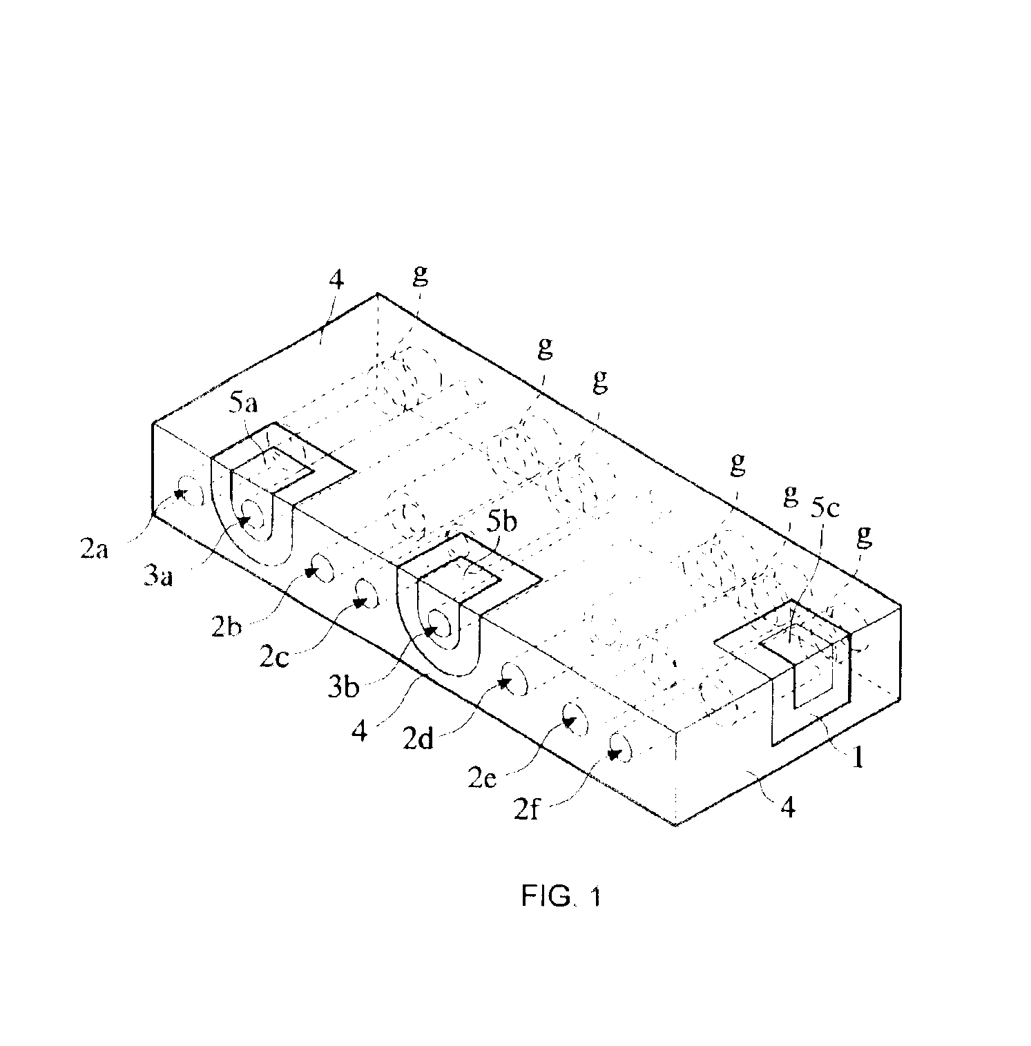
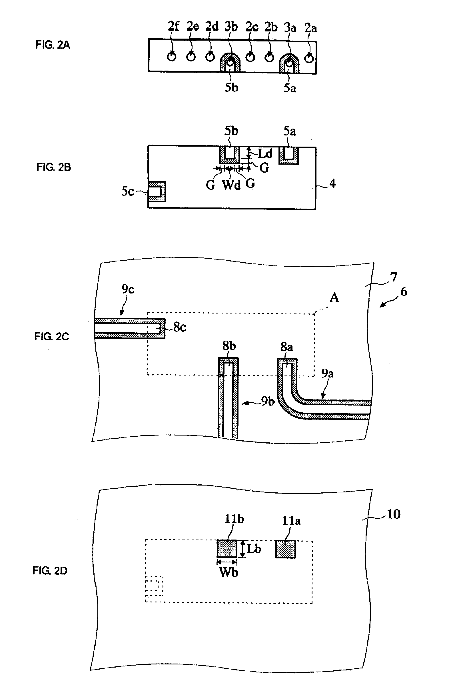
[0032]FIG. 1 is a perspective view of the dielectric duplexer according to a first embodiment. In FIG. 1, a dielectric block 1 in the form of a substantially rectangular parallelepiped is shown. Inside the dielectric block 1, resonator holes 2a to 2f and excitation holes 3a and 3b are provided so as to extend from one surface of the dielectric block 1 to the other surface opposite thereto. On the inner surface of the resonator holes 2a to 2f and the excitation holes 3a and 3b, an inner conductor is formed. An outer conductor 4 is formed on the outer surface (six faces) of the dielectric block 1. Furthermore, input-output terminals 5a to 5c, which are separated from the outer conductor 4, are formed at fixed locations on the outer surface of the dielectric block 1.

[0033]While the inner conductor is formed on the inner surface of the resonator holes 2a t...

second embodiment

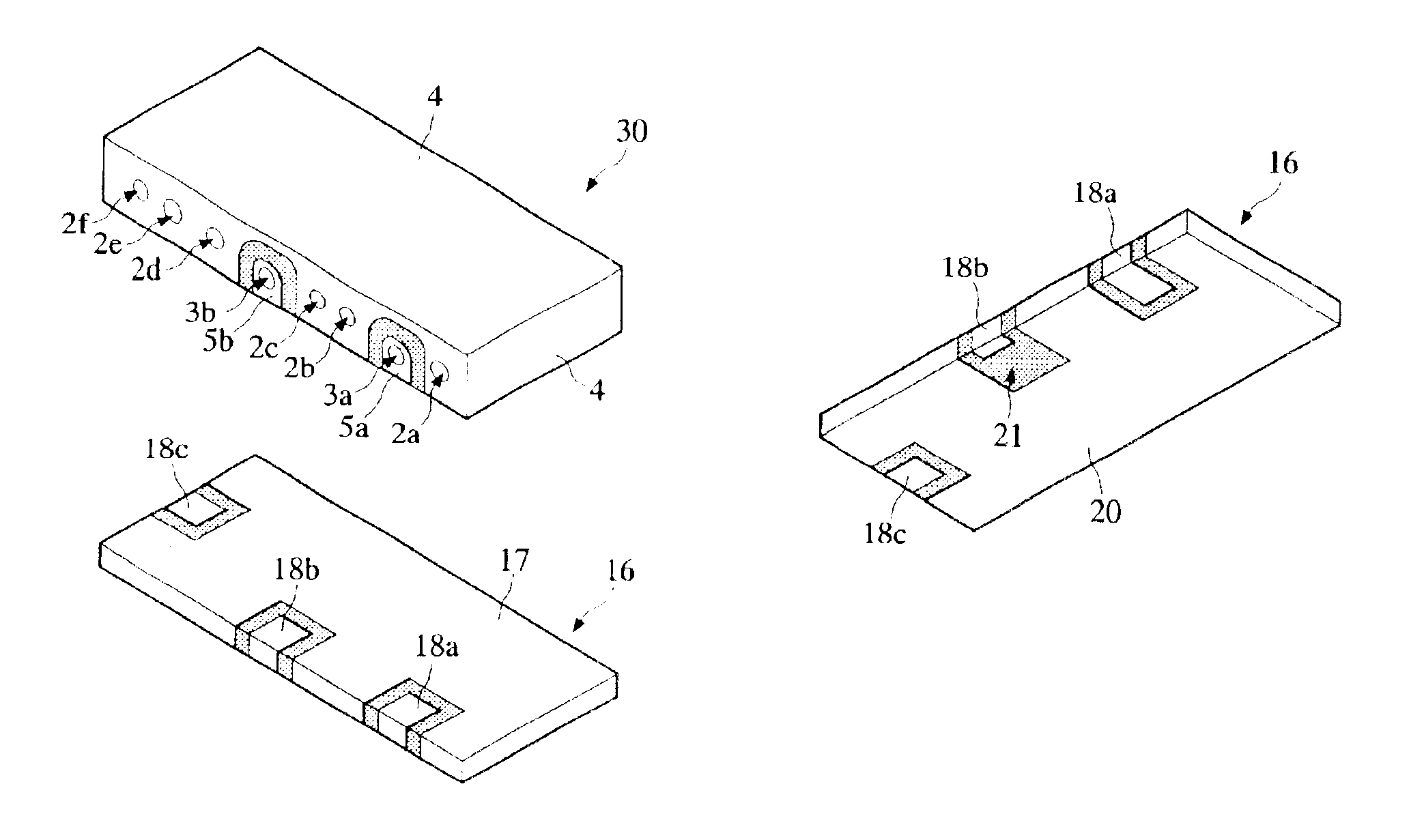
[0047]Next, the structure of a dielectric duplexer device according to the present invention is described with reference to FIGS. 5A, 5B, and 6.

[0048]The dielectric duplexer device contains a dielectric duplexer having the related structure and a new adapter substrate.

[0049]FIG. 5A is an exploded perspective view of the dielectric duplexer device and FIG. 5B is a perspective view as seen from the bottom side, that is, the mounting surface to the mounting substrate, of the adapter substrate. Here, a dielectric duplexer 30 is shown and has the same structure as shown in FIG. 1. That is, the resonator holes 2a to 2f and excitation holes 3a and 3b are provided in the dielectric block in the form of a substantially rectangular parallelepiped. The input-output terminals 3a and 3b and the outer conductor 4 are formed on the outer surface of the dielectric block.

[0050]An adapter substrate 16 is shown in the drawings and input-output electrodes 18a, 18b, and 18c are formed from the upper sur...

third embodiment

[0056]Next, the structure of a communication device according to the present invention is described with reference to FIG. 7.

[0057]In FIG. 7, a transmission-reception antenna ANT, a duplexer DPX, bandpass filters BPFa and BPFb, amplifiers AMPa and AMPb, mixers MIXa and MIXb, an oscillator OSC, and a frequency synthesizer SYN are shown.

[0058]The mixer MIXa mixed a transmission intermediate-frequency signal IF and a signal output from the frequency synthesizer SYN, the bandpass filter BPFa allows only a mixed output signal in the transmission frequency band from the mixer MIXa to pass through, and the amplifier AMPa amplifies the mixed output signal to transmit the signal through the duplexer DPX from the antenna ANT. The amplifier AMPb amplifies a reception signal from the duplexer DPX. The bandpass filter BPFb allows only a reception signal in the reception frequency band output from the amplifier AMPb to pass through. The mixer MIXb mixes a signal output from the frequency synthesi...


PUM


Abstract

An excitation hole is provided inside a dielectric block and, on the outer surface of the dielectric block, an input-output terminal electrically connected to an inner conductor inside the excitation hole is formed at one end portion of the excitation hole. A grounding-electrode-free portion is provided on the surface opposite to an input-output electrode of a mounting substrate with which the input-output terminal makes contact. Thus, the electric field strengths in upward and downward directions toward an outer conductor of the dielectric block from the excitation hole are balanced to suppress spurious TE-mode signals, etc.

Description

BACKGROUND OF THE INVENTION[0001]1. Field of the Invention[0002]The present invention relates to a dielectric filter, dielectric filter device, dielectric duplexer, and a communication device having these, which are applied to, for example, high-frequency circuits for mobile communication terminals.[0003]2. Description of the Related Art[0004]The mounting structure of a related dielectric duplexer is shown in FIGS. 8A to 8D. FIG. 8A is a front view of the dielectric duplexer and FIG. 8B is its bottom view. Inside a dielectric block in the form of a substantially rectangular parallelepiped, resonator holes 2a to 2f and excitation holes 3a and 3b are provided. On the outer surface of the dielectric block, an outer conductor 4 and input-output terminals 5a, 5b, and 5c are formed. The input-output terminals 5a and 5b are electrically connected to one end portion of the inner conductor formed on the inner surface of the excitation holes 3a and 3b, respectively.[0005]FIG. 8C is a top view...

Claims


Application Information

Patent Timeline
Patent Type & Authority Patents(United States)
IPC IPC(8): H01P1/213H01P1/20H01P1/205H01P1/212H01P5/08
CPCH01P1/2136H01P1/2056
Inventor YONEKURA, HIROSHIMIYAMOTO, HIROFUMI
Owner MURATA MFG CO LTD
Why Eureka
Try Eureka