4H-SiC metal semiconductor field effect transistor (MSFET) with multi-recess buffer layer

A field effect transistor and metal semiconductor technology, which is applied in the field of 4H-SiC metal semiconductor field effect transistors, can solve problems such as the large influence of saturation leakage current, and achieve the advantages of increasing breakdown voltage, alleviating electric field strength, and improving gate transconductance. Effect

Active Publication Date: 2017-06-30
XIDIAN UNIV
View PDF5 Cites 2 Cited by
  • Summary
  • Abstract
  • Description
  • Claims
  • Application Information

AI Technical Summary

Problems solved by technology

[0005] Chinese patent (application number 201410181931.6) discloses 4H-SiC metal-semiconductor field effect transistor, but its structure has a great influence on the saturation leakage current while increasing the breakdown voltage

Method used


Image

  • 4H-SiC metal semiconductor field effect transistor (MSFET) with multi-recess buffer layer

Examples


Embodiment 1

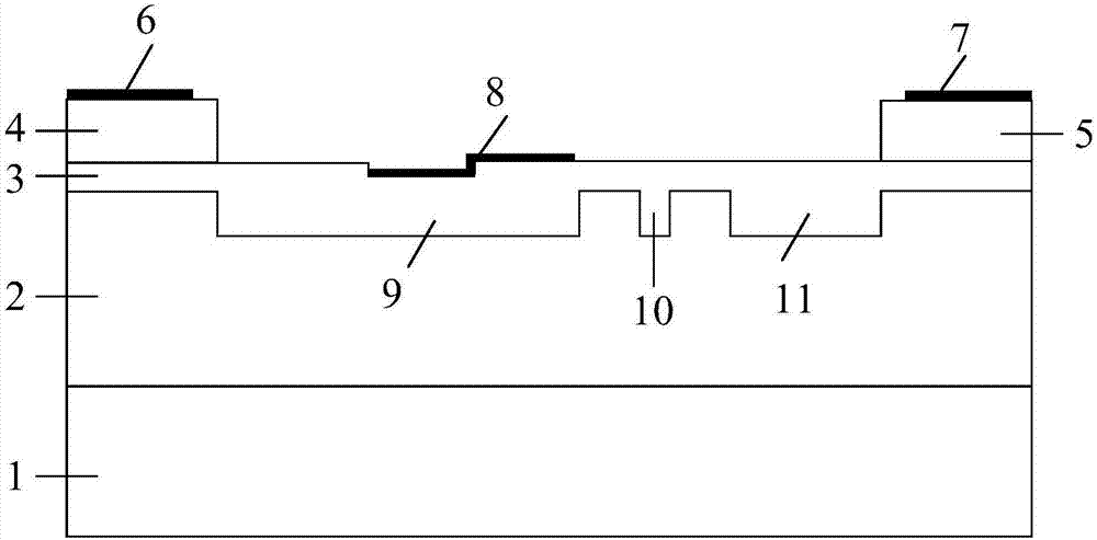
[0025] A 4H-SiC metal-semiconductor field-effect transistor with multiple recessed buffer layers, comprising a 4H-SiC semi-insulating substrate (1), a P-type buffer layer (2), and an N-type channel layer (3) from bottom to top, The two sides of the N-type channel layer (3) are respectively a source cap layer (4) and a drain cap layer (5), and the surfaces of the source cap layer (4) and the drain cap layer (5) are respectively source electrodes ( 6) and the drain electrode (7), the gate electrode (8) is formed on the side of the N-type channel layer (3) and close to the source cap layer, and the upper end surface of the buffer layer is provided below the gate electrode and the gate source The first buffer layer recessed area (9), the second buffer layer recessed area (10) is provided on the side near the gate under the gate drain, and the third buffer layer is provided on the side near the drain cap layer below the gate drain Depressed area (11).

Embodiment 2

[0027] In this embodiment, the depth of the P-type buffer layer (2) is 0.65 μm, and the first buffer layer recessed area (9), the second buffer layer recessed area (10), and the third buffer layer recessed area (11) The depths are all 0.15 μm.

[0028] The remaining technical solutions of this embodiment are consistent with Embodiment 1.

Embodiment 3

[0030] In this embodiment, the depth of the P-type buffer layer (2) is 0.6 μm, and the first buffer layer recessed area (9), the second buffer layer recessed area (10), and the third buffer layer recessed area (11) The depths are all 0.1 μm.

[0031] The remaining technical solutions of this embodiment are consistent with Embodiment 1.


PUM


Abstract

The invention discloses a 4H-SiC MSFET with a multi-recess buffer layer, belongs to the technical field of field effect transistors, and aims at improving the breakdown voltage and transconductance parameter of the field effect transistor and improving a DC characteristic. The MSFET comprises a 4H-SiC semi-insulating substrate, a P type buffer layer and an N type trench layer from bottom to top, a source cap layer and a drain cap layer are arranged at the two sides of the N type trench layer respectively, a source electrode and a drain electrode are arranged in the surfaces of the source cap layer and the drain cap layer respectively, a gate electrode is formed on the N type trench layer at the side close to the source cap layer, the upper end surface of the buffer layer is provided with three buffer-layer recess regions respectively in positions under the gate electrode and a gate source, under a gate-drain at the side close to the gate electrode and under the gate-drain at the side close the drain cap layer, the depths of the three buffer-layer recess regions are all 0.15 micron, and the lengths of the three buffer-layer recess regions are 1.2, 0.1 and 0.5 microns respectively.

Description

technical field [0001] The invention belongs to the technical field of field effect transistors, and in particular relates to a 4H-SiC metal semiconductor field effect transistor with multi-sag buffer layers. Background technique [0002] Silicon carbide (SiC) has attracted people's attention due to its excellent electrical properties such as wide band gap, high critical electric field, high saturation drift velocity and high thermal conductivity, and has become the third-generation semiconductor material. These excellent properties make silicon carbide (SiC) often used in working conditions such as high pressure, high temperature, high frequency, and high power. SiC plays a major role in the application of microwave power devices, especially metal semiconductor field effect transistors (MESFETs), and has become a research hotspot in the field of microwave power devices in recent years. [0003] Among power devices in the microwave frequency band, 4H-SiC MESFETs have extrem...

Claims


Application Information

Patent Timeline
Patent Type & Authority Applications(China)
IPC IPC(8): H01L29/78H01L29/06
CPCH01L29/0611H01L29/78
Inventor 贾护军吴秋媛杨银堂柴常春
Owner XIDIAN UNIV
Why Eureka
Try Eureka