Method for creating waveguides in multilayer ceramic structures and a waveguide having a core bounded by air channels

a multi-layer ceramic and waveguide technology, applied in waveguides, electrical equipment, antennas, etc., can solve the problems of large physical size compared to the rest of the circuit unit to be manufactured, increased cost and failure risk, and difficult integration of their manufacture into the manufacturing of the circuit unit as a whol

Inactive Publication Date: 2005-06-21
NOKIA CORP
View PDF6 Cites 128 Cited by
  • Summary
  • Abstract
  • Description
  • Claims
  • Application Information

AI Technical Summary

Benefits of technology

[0007]The objective of the invention is to accomplish a waveguide structure implemented with multilayer ceramics, by which the above-mentioned drawbacks of the prior art guide structure can be reduced.
[0016]The invention has the advantage that the waveguide can be manufactured simultaneously with other components manufactured with the multilayer ceramic technique.
[0017]In addition, the invention has the advantage that the feeding arrangement of the waveguide can be implemented with the same multilayer ceramic technique.
[0018]The invention also has the advantage that the manufacturing costs of a waveguide manufactured with the method are lower than those of a waveguide made of separate components and joined to the structure in a separate step.
[0019]Furthermore, the invention has the advantage that it has a good EMC protection as compared to a strip line, microstrip or coplanar conductor.

Problems solved by technology

However, the problem with these waveguides is the large physical size compared to the rest of the circuit unit to be manufactured, and the fact that it is difficult to integrate their manufacture into the manufacture of the circuit unit as a whole.
These waveguides must be joined to the circuit unit mechanically either by soldering or by some other mechanical joint in a separate step, which increases costs and the risk of failure.
The temperature used in the LTCC technique is around 850° C. and in the HTCC technique around 1600° C. However, the problem of microstrips, strip lines and coplanar conductors made with these techniques is the high attenuation per unit of length, low power margin and relatively low ElectroMagnetic Compatibility (EMC).
These problems limit the use of these conductor structures in the applications where the above-mentioned properties are needed.

Method used


Image

  • Method for creating waveguides in multilayer ceramic structures and a waveguide having a core bounded by air channels
  • Method for creating waveguides in multilayer ceramic structures and a waveguide having a core bounded by air channels
  • Method for creating waveguides in multilayer ceramic structures and a waveguide having a core bounded by air channels

Examples


first embodiment

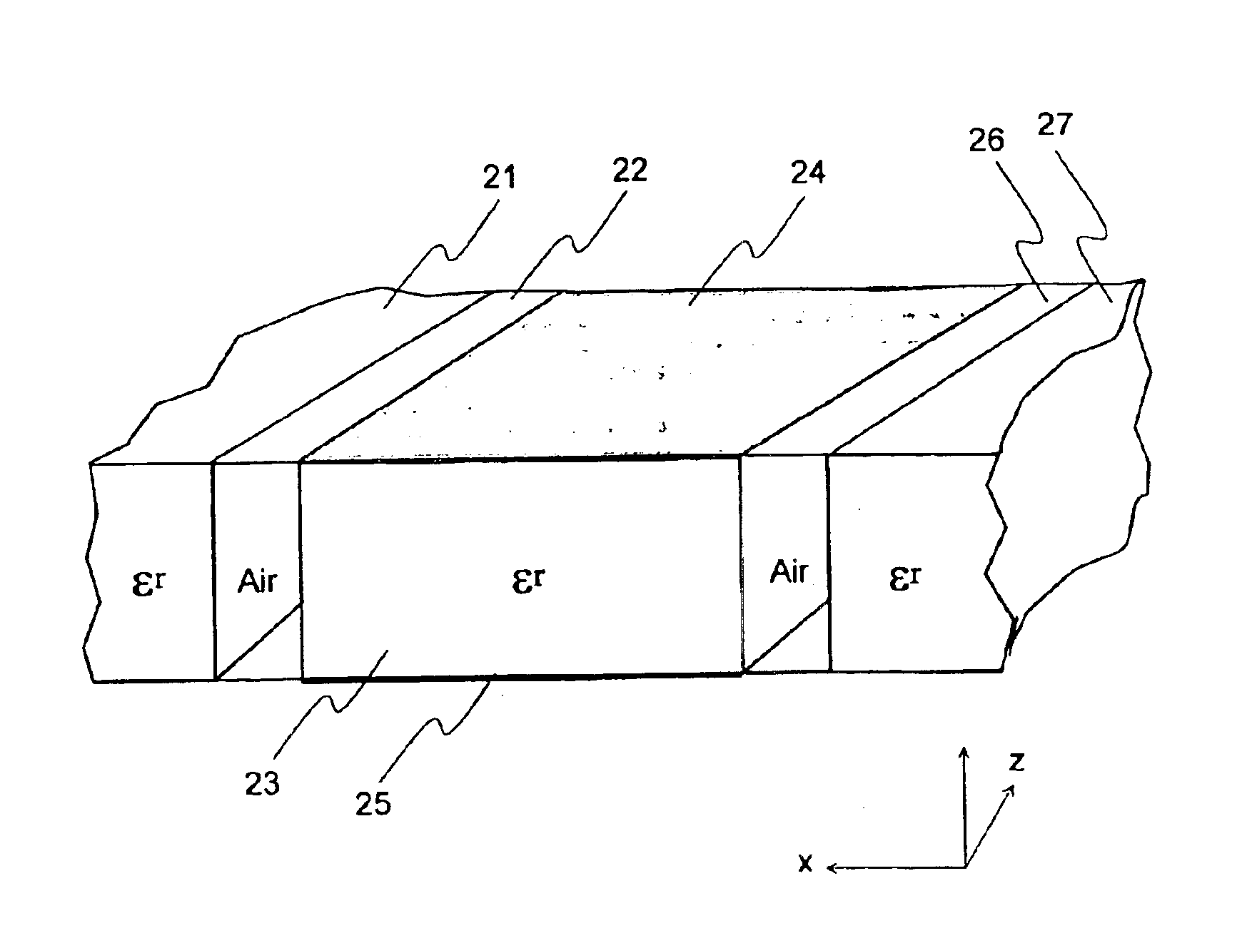
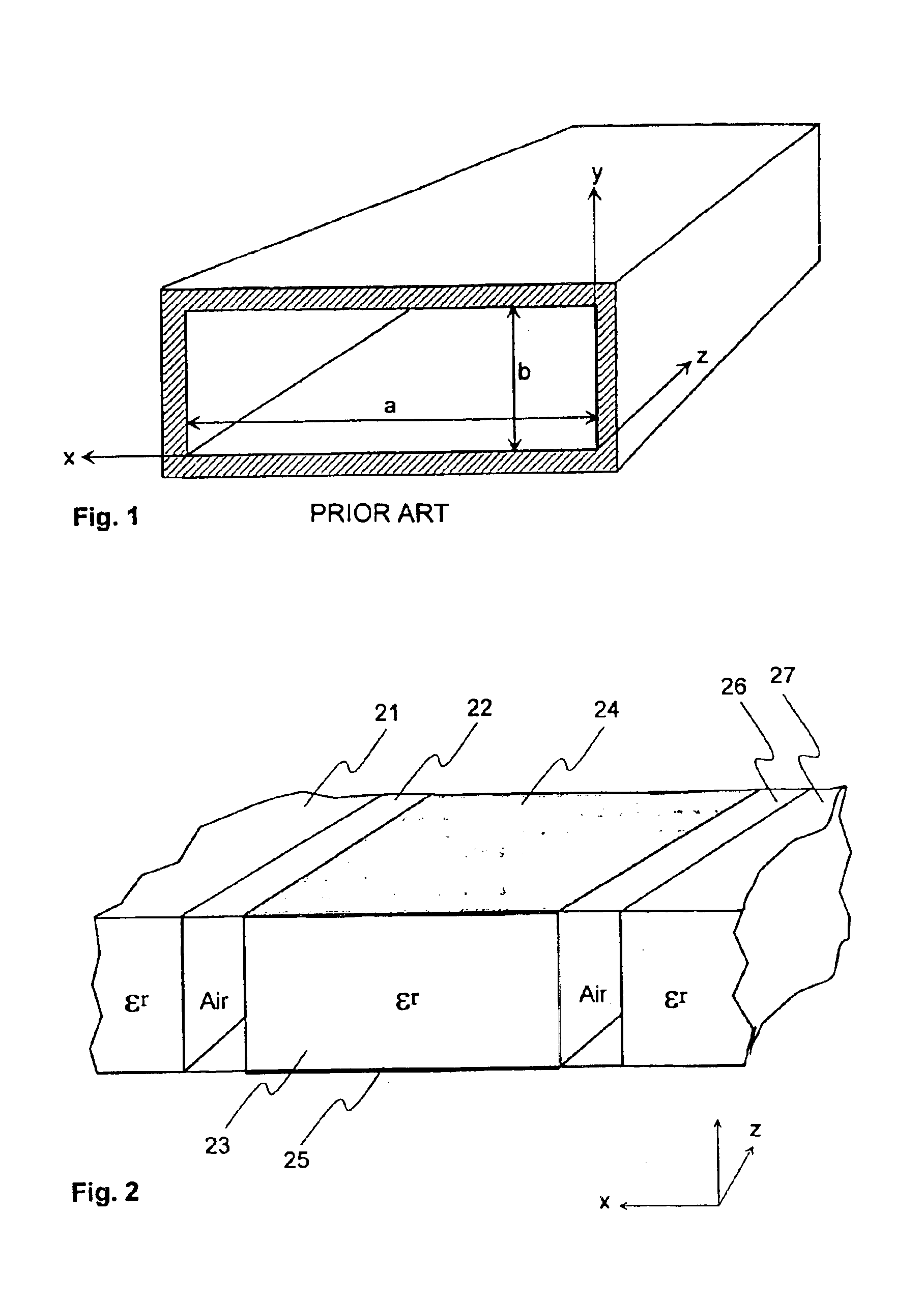
[0032]FIG. 2 shows an example of a waveguide according to the invention, implemented with the multilayer ceramic technique. The structure shown in FIG. 2 is part of a larger circuit structure implemented with the multilayer ceramic technique, which is not shown in its entirety in the drawing. The waveguide structure is surrounded on both sides by the structures 21 and 27 shown in the drawing, which consist of several green tapes. The permittivity εr of the ceramic material used in them is clearly higher than the permittivity of air, which is of the magnitude 1, as is well known. Other parts of the structure, which are both above and below the waveguide structure shown in the drawing, viewed in the direction of the y-axis, consist mainly of the same ceramic material. The core part 23 of the waveguide consists of the same ceramic material as the rest of the circuit structure. The width of the waveguide in the direction of the x-axis is limited by air-filled cavities 22 and 26 essentia...

second embodiment

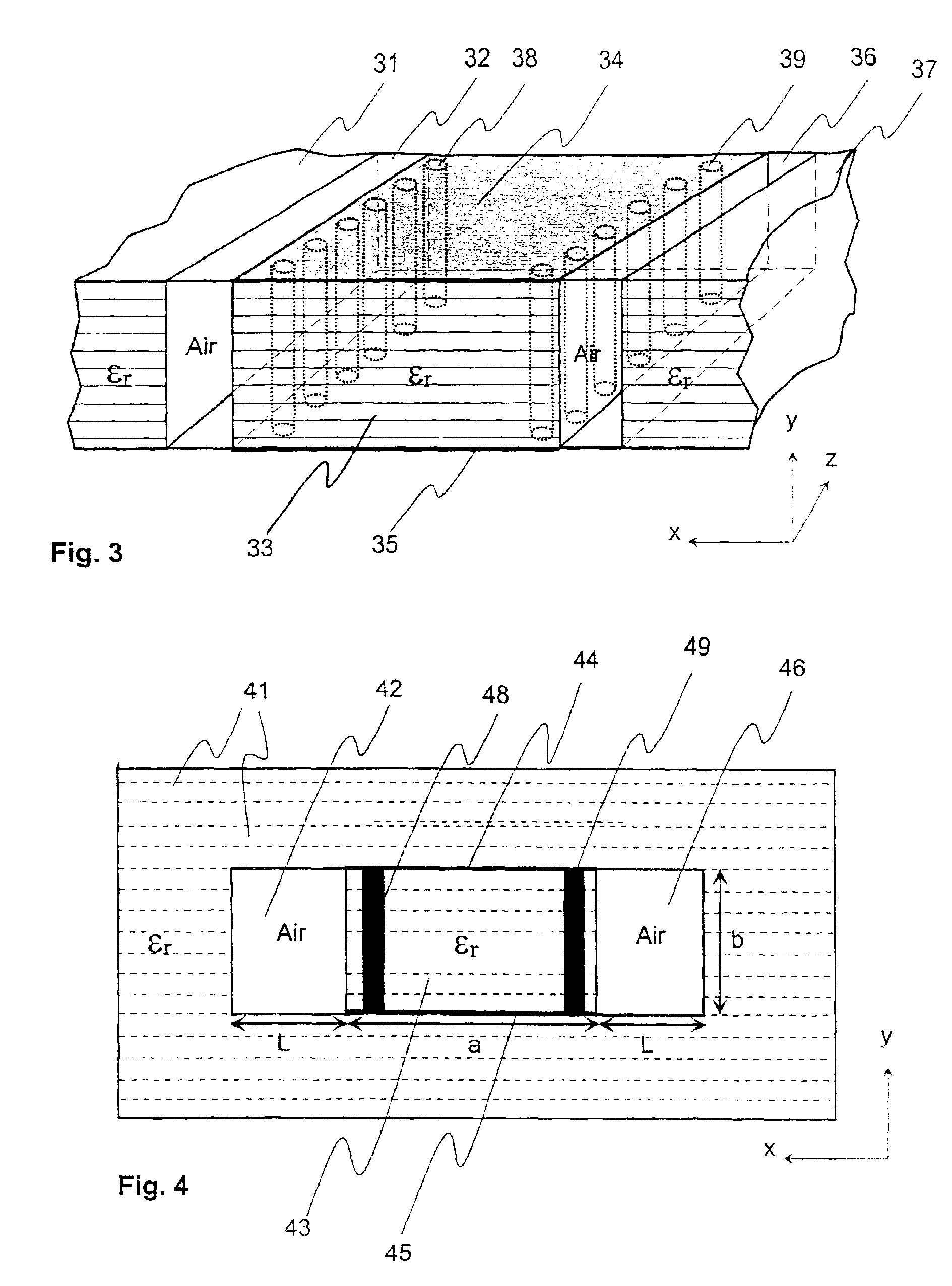
[0034]FIG. 3 shows an example of a waveguide according to the invention. The structure shown in FIG. 3 is part of a larger structure implemented with the multilayer ceramic technique, which is not shown in its entirety in the drawing. The waveguide structure is surrounded on both sides by the structures 31 and 37 shown in the drawing, which consist of several green tapes. The permittivity εr of the ceramic material used in them is clearly higher than the permittivity of air, which is of the magnitude 1. Other parts of the structure, which are both above and below the waveguide structure shown in the drawing, viewed in the direction of the y-axis of the drawing, also consist mainly of the same ceramic material. The core part 33 of the waveguide consists of the same ceramic material as the rest of the circuit structure. The width of the waveguide in the direction of the x-axis is limited by two essentially parallel impedance discontinuities, which are formed of via posts 38 and 39 in ...


PUM

PropertyMeasurementUnit
thickaaaaaaaaaa
cut-off frequencyaaaaaaaaaa
permittivity εraaaaaaaaaa

Abstract

The invention relates to a waveguide manufacturing and a waveguide manufactured with the method, which can be integrated into a circuit structure manufactured with the multilayer ceramic technique. The core part (23, 33, 43, 53a, 53b, 53c) of the waveguide is formed by a unit assembled of ceramic layers, which is limited in the yz plane by two impedance discontinuities and in the xz plane by two planar surfaces (24, 25, 34, 35, 54a, 54c, 55a, 55b, 55c) made of conductive material. The conductive surfaces can be connected to each other by vias made of conductive material (38, 39, 48, 49). The waveguide manufactured with the method according to the invention is a fixed part of the circuit structure as a whole.

Description

PRIORITY CLAIM[0001]This is a national stage of PCT application No. PCT / FI00 / 00635, filed on Jul. 10, 2000. Priority is claimed on that application, and on patent application No. 991585 filed in Finland on Jul. 9, 1999.FIELD OF THE INVENTION[0002]The invention relates to a method for creating waveguides in circuit board units manufactured with the multilayer ceramic technique, in which method the dimensions and structural directions of the circuit board units can be defined by means of x, y and z axes perpendicular to each other, and the circuit board unit is assembled of separate ceramic layers, the permittivity εr of which is higher than the corresponding value of air, and in which layers cavities and holes of the desired shape can be made, and on the surface of which ceramic layer a conductive material can be printed at the desired location by silk screen printing, and the circuit board unit is completed by exposing the unit to a high temperature.[0003]The invention also relates ...

Claims


Application Information

Patent Timeline
Patent Type & Authority Patents(United States)
IPC IPC(8): H01P3/12H01P3/00H01P11/00
CPCH01P3/121Y10T29/49016
Inventor SALMELA, OLLIKEMPPINEN, ESASOMERMA, HANSIKALAINEN, PERTTIKOIVISTO, MARKKU
Owner NOKIA CORP
Why Eureka
Try Eureka