Method and system for estimating microelectronic fabrication product yield

a technology of microelectronic fabrication and product yield, which is applied in forecasting, instruments, data processing applications, etc., can solve the problems of not being readily implemented in products, and achieve the effect of being ready for commercialization

Inactive Publication Date: 2005-06-21
TAIWAN SEMICON MFG CO LTD
View PDF5 Cites 1 Cited by
  • Summary
  • Abstract
  • Description
  • Claims
  • Application Information

AI Technical Summary

Benefits of technology

[0021]The method of the present invention and the system of the present invention are readily commercially implemented.

Problems solved by technology

In that regard, methods and systems for determining microelectronic fabrication product yield when fabricating microelectronic fabrication products are not often readily implemented in the art of microelectronic fabrication insofar as they are often dependent upon complex, cumbersome and intricate microelectronic fabrication product yield modeling equations.

Method used


Image

  • Method and system for estimating microelectronic fabrication product yield
  • Method and system for estimating microelectronic fabrication product yield
  • Method and system for estimating microelectronic fabrication product yield

Examples


Embodiment Construction

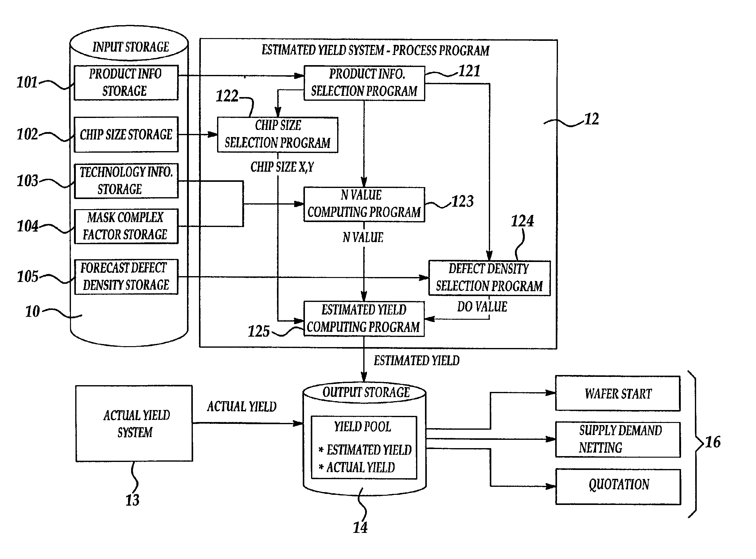
[0026]There is provided by the present invention a method and a system for estimating a microelectronic fabrication product yield when fabricating a microelectronic fabrication product, wherein the microelectronic fabrication product yield is efficiently estimated.

[0027]The method of the present invention and the system of the present invention realize the foregoing objects with respect to a new microelectronic fabrication product to be fabricated within at least one microelectronic fabrication facility, through use of a mathematic algorithm which operates in part through correlation with historic microelectronic fabrication production data for fabricating an existing series of microelectronic fabrication products fabricated within the at least one microelectronic fabrication facility.

[0028]While the preferred embodiment of the present invention provides particular value within the context of estimating semiconductor integrated circuit microelectronic fabrication product yield for a...


PUM


Abstract

Within a method for estimating a microelectronic fabrication product yield and a system for estimating the microelectronic fabrication product yield there is employed a specific mathematic algorithm for estimating yield of a new microelectronic fabrication product within at least one microelectronic fabrication facility. The specific algorithm is solved incident to parametric data correlation with existing production data within the at least one microelectronic fabrication facility.

Description

BACKGROUND OF THE INVENTION[0001]1. Field of the Invention[0002]The present invention relates generally to methods and systems for fabricating microelectronic fabrication products. More particularly, the present invention relates to methods and systems for estimating microelectronic fabrication product yield when fabricating microelectronic fabrication products.[0003]2. Description of the Related Art[0004]Microelectronic fabrications are formed from microelectronic substrates over which are formed patterned microelectronic conductor layers which are separated by microelectronic dielectric layers.[0005]Desirable in the art of microelectronic fabrication for use when fabricating microelectronic fabrications are methods and systems for determining microelectronic fabrication product yield when fabricating microelectronic fabrication products. Methods and systems for determining microelectronic fabrication product yield when fabricating microelectronic fabrication products are desirable...

Claims


Application Information

Patent Timeline
Patent Type & Authority Patents(United States)
IPC IPC(8): G06Q10/00G06Q50/00G06Q10/04G06Q50/04
CPCG06Q50/04G06Q10/04Y02P90/30
Inventor LIAO, YUN-WEIKA, REGINACHU, MEI-LING
Owner TAIWAN SEMICON MFG CO LTD
Why Eureka
Try Eureka